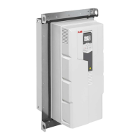
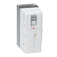
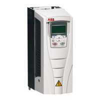
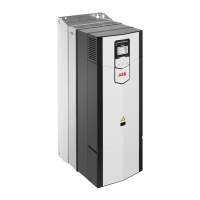
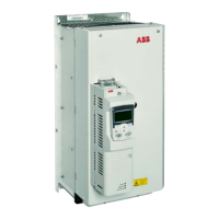
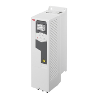
Overview of power and control connections
The logical diagram below shows the power connections and control interfaces
of the drive.
L1
L2
L3
PE
T1/U
T2/V
T3/W
M
3 ~
L1
L2
L3
PE
R-
UDC+
R+
UDC-
1
2
..........
..........
..........
..........
..........
..........
3
1)
1)
4
Option slot 1 for optional fieldbus adapter modules1
Option slot 2 for optional I/O extension modules2
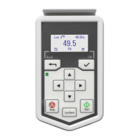
Panel port3
du/dt or common mode filter (optional), see Common mode, d
u
/d
t
and sine fil-
ters (page 461).
4
1)
Not in all frame sizes
48 Operation principle and hardware description
 Loading...