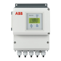
-in module 2 DIP switch
Assigning of DIP switches
DIP switch 1:
Releases the simulation of the AI function blocks.
DIP switch 2:
Hardware write protection for write access via bus (locks all blocks).
DIP switch 1 2 3 ... 10
status Simulation Mode Write protect no function
Off Disabled Disabled no function
On Enabled Enabled no function
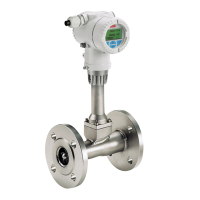
Bus address settings
The bus address is automatically allocated at the FF via LAS (link active scheduler). For
address detection, a unique number is used (DEVICE_ID). This number is a combination of
manufacturer ID, device ID and device serial number.
The behavior when switching on the unit corresponds to Draft DIN IEC / 65C / 155 / CDV of
June 1996.
The average current draw of the unit is 10 mA. The voltage on the bus line must lie in the range
of 9 … 32 V DC.
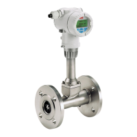
Important
The upper limit of the current is electronically limited. In the event of an error, the integrated
FDE function (Fault Disconnection Electronic) integrated in the device ensures that the current
consumption can rise to a maximum of 13 mA.
 Loading...