S19 Maintenance Guide
5
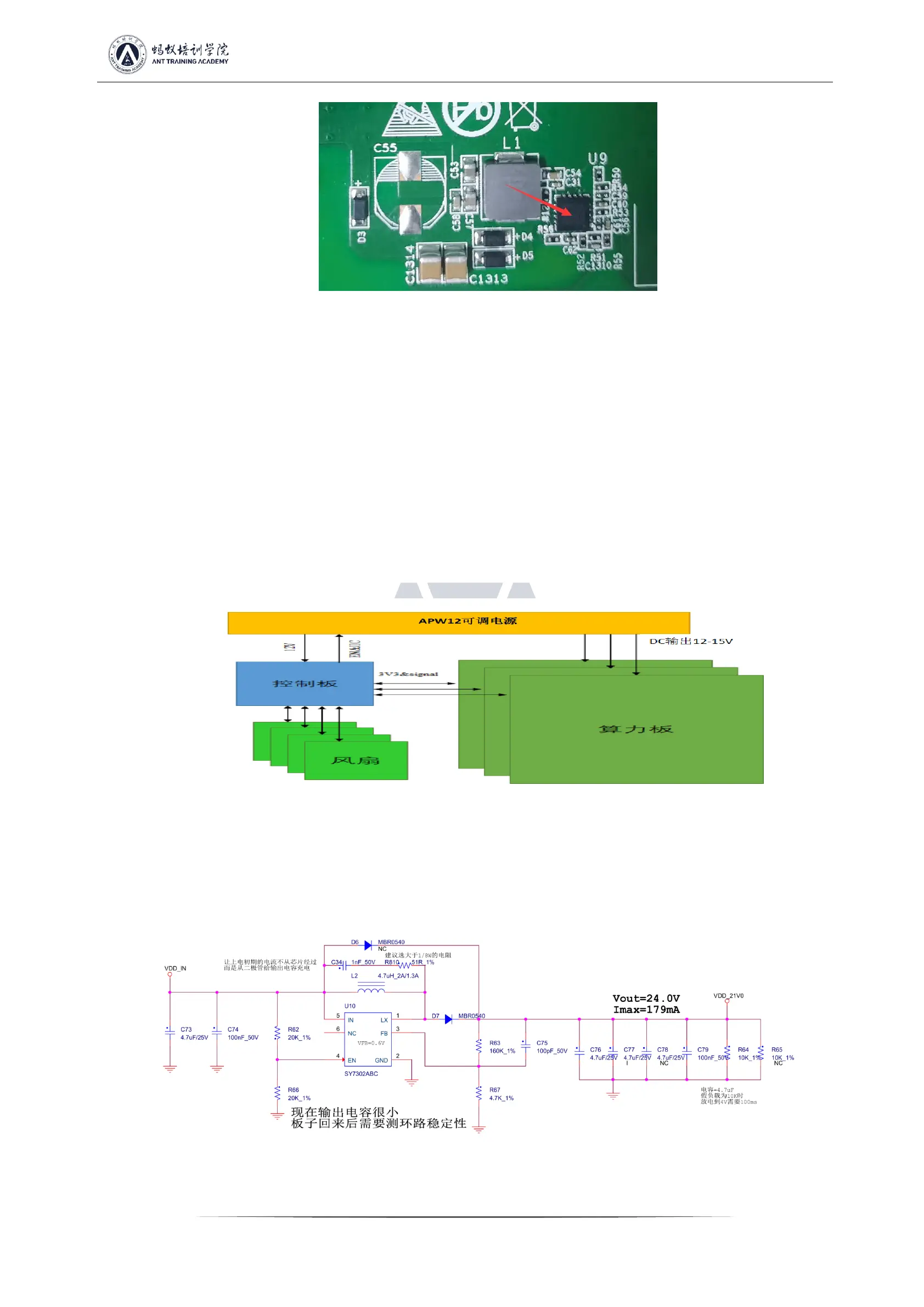
Figure 4-5
3. Signal trend of S19 chip:
1) CLK (XIN) signal flow direction, generated by Y1 25M oscillator, transmitting from chip 01 to chip 76; voltage of 0.7V-1.3V;
2) TX (CI, CO) signal flow direction, from IO port 7 pin (3.3V) into IC U2 through level conversion, and then transmitted from chip 01 to
chip 76; the voltage is 0V when the IO signal is not inserted, and the voltage is 1.8V during operation;
3) RX (RI, RO) signal flow direction, from chip 76 to chip 01, return to the signal cable terminal pin 8 through U1 and then return to the
control board; when the IO signal is not inserted, the voltage is 0.3V, and the voltage will be 1.8V during computing;
4) BO (BI, BO) signal flow direction, from chip 01 to chip 76; the multimeter measurement value is 0V;
5) The RST signal flow is from pin 3 of the IO port, and then is transmitted from chip 01 to chip 76; if no IO signal is inserted and
equipment is in standby, voltage is 0V, 1.8V when computing;
4. Whole machine architecture:
The whole machine is mainly composed of 3 hashboards, 1 control board, APW12 power supply, and 4 cooling fans, as shown in Figure 4-
6.
Figure 4-6
V. Common faults and troubleshooting steps of the hashboard
1. Phenomenon: single board test detection chip is 0 (PT1/PT2 stations)
First step: check the power output first, please check the circled part in Figure 5-1.
 Loading...