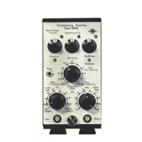
resistance
is
47
kQ
at
25°C,
falling down
to
1.2
kQ
at
125°C.
It
is
part
of
the base biasing
network
of
the
gating transistor.
The
circuit
is
shown
in
Fig.4.2.
-9V
/f12ooS
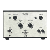
Fig.4.2. Temperature sensitive gating
circuit
of
2706
For normal working
temperatures
(around
80°C
on
the
heat
sink)
the
DC
collector-emitter voltage
is
kept
to
a value allowing AC signals
to
be
passed
to
the
gate
output.
If
temperature
rises,
the
thermistor
resistance
reduces, causing
the
base-emitter voltage
to
increase and therefore
the
collector-emitter voltage
is
reduced. This introduces a limitation on
the
voltage allowed
to
go pass
the
gate
without
clipping
(the
peak voltage being
limited
to
the
collector-emitter voltage). Clipping will be indicated by
the
CLIPPING lamp. If
temperature
on
the
heat
sink
is
increased
further
up
to
125°C,
the
collector-emitter voltage
is
reduced
to
zero and
the
signal
is
grounded and therefore does
not
reach
the
power
section.
When
the
heat
sink
temperature
reduces,
the
Power Amplifier will
automatically become operative again.
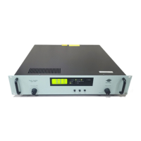
4.5
CHARACTERISTICS
4.5.1. Power
output
capacity
The
overall voltage gain
of
the
Power Amplifier
is
40
dB ± 1
dB
at
1 kHz.
Output
voltage
is
limited
to
5 Amps RMS
or
1.8
Amps
RMS. Power
output
capacity
is
75
VA into a 3 n load. For loads above 3 n power
is
limited
by
the
maximum voltage available ( 15 Volts RMS). Below 3 n, it
is
limited
by
10
•
 Loading...