— 12 —
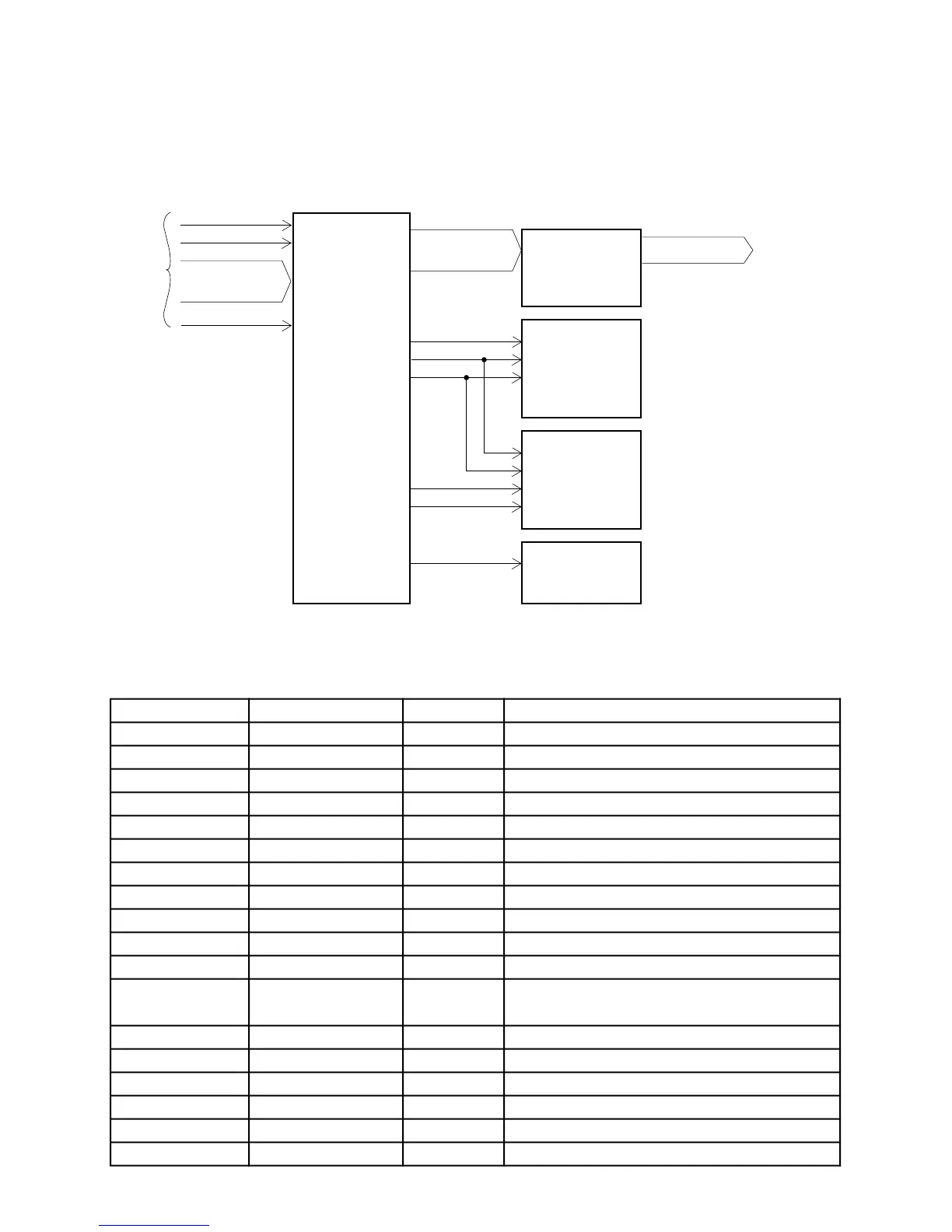
GATE ARRAY (LSI17: UPD65611GB)
The gate array provides chip enable signals for DSP, Key Controller, and Working Storage RAM. The LSI
also generates scan signals of the button switches with K0O and K0C signals from the CPU.
KO0 ~ KO15
To CPU
KI1 ~ KI4
A4 ~ A15
Gate Array
UPD65611GB
LSI17
Button Switch
Matrix
K0O
K0C
HGB
CLKA
SAMPB
CWRB
CRDB
CCSB
CKI
CS
LSIB
WRAB
RDAB
CCSB
CWRB
CRDB
CLK
DSP
HG51B155FD
LSI11
Key Controller
HG52E35P
LSI16
Working Storage RAM
TC55257DFL-70L
LSI15
From CPU
Each pin function of the LSI is listed below.
Pin No. Terminal In/Out Function
1 K0C In Primary signal for KO0 ~ KO15
2 APOB In APO signal from CPU
3 RDB In Read enable signal from CPU
4 WRB In Write enable signal from CPU
5 WRAB Out Write enable signal for DSP and Key Controller
6 CLK In Clock pulse from CPU
7 LSIB Out DSP chip select signal
8 RDAB Out Read enable to DSP and Key Controller
9 RESET Out DSP and Key Controller reset signal
10 LED1 — Not used
11 LED0 — Not used
17 GND In Ground (0 V) source
23 NC — Not used
24 GND In Ground (0 V) source
25 CLKA Out 16 MHz Clock pulse for Key Controller
26 GND In Ground (0 V) source
27 HGB Out Key Controller chip select signal
12 ~ 16, 18 ~ 22 Out Button switch scan signalsKO0 ~ KO9