DS1821
13 of 18
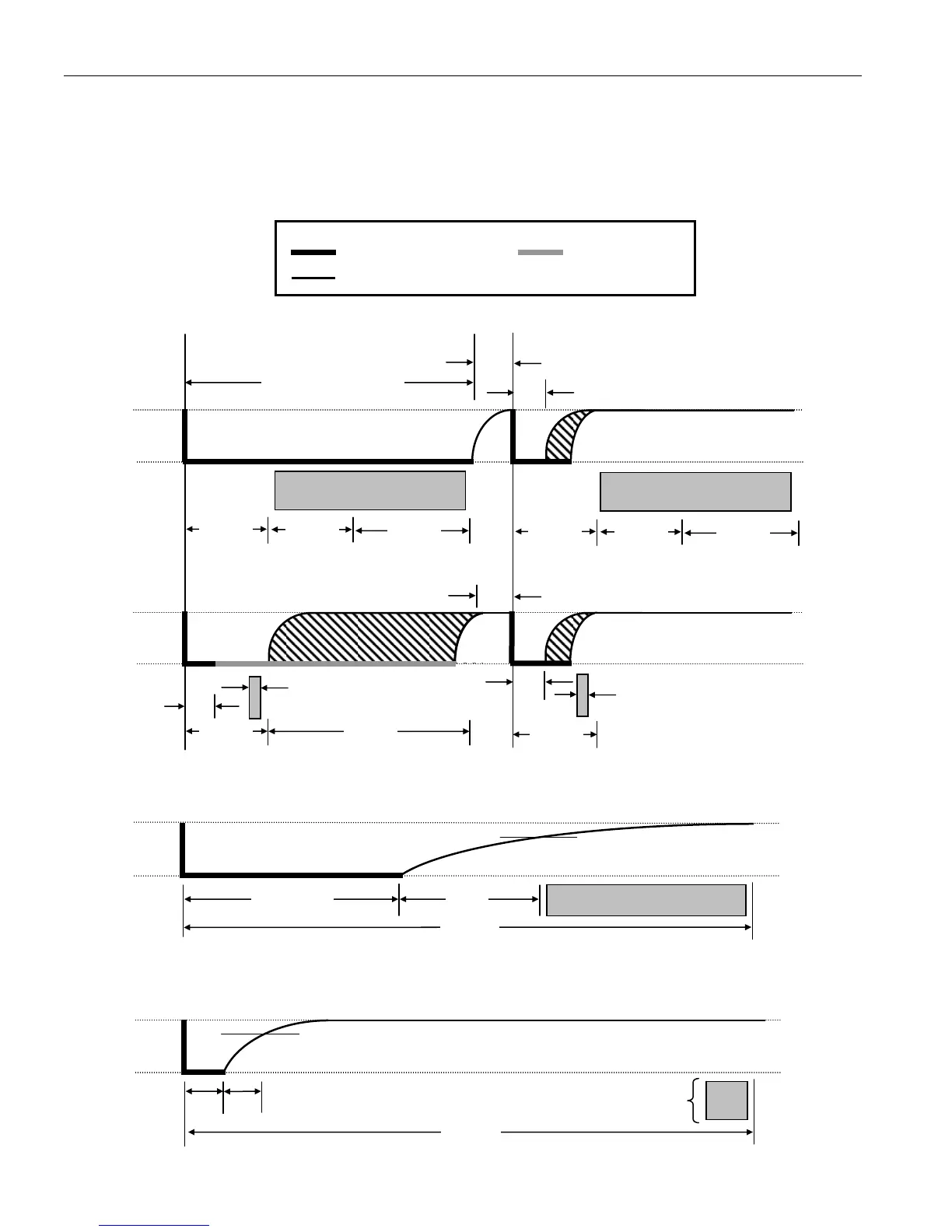
Figure 9 illustrates that the sum of T
INIT
, T
RC
, and T
SAMPLE
must be less than 15 μs for a read time slot.
Figure 10 shows that system timing margin is maximized by keeping T
INIT
and T
RC
as short as possible
and by locating the master sample time during read time slots towards the end of the 15 μs period.
READ/WRITE TIME SLOT TIMING DIAGRAM Figure 8
DETAILED MASTER READ 1 TIMING Figure 9
RECOMMENDED MASTER READ 1 TIMING Figure 10
V
DD
GND
1-WIRE BUS
15
s
VIH of Master
T
RC
T
INT
> 1 μs
Master samples
V
DD
GND
1-WIRE BUS
15
s
VIH of Master
T
RC
=
small
T
INT
=
small
Master samples
LINE TYPE LEGEND (Figure 8, Figure 9 and Figure 10)
Bus master pulling low DS1821 pulling low
Resistor pullup
45 μs
15 μs
V
DD
GND
1-WIRE BUS
60 μs < T
X
“0” < 120
1 μs < T
REC
<
DS1821 samples
MIN TYP MAX
15 μs
30
s
> 1
s
MASTER WRITE “0” SLOT MASTER WRITE “1” SLOT
DS1821 samples
MIN TYP MAX
V
DD
GND
1-WIRE BUS
15
s
MASTER READ “0” SLOT MASTER READ “1” SLOT
Master samples
Master samples
START
OF SLOT
START
OF SLOT
> 1
s
1 μs < T
REC
<
15 μs
15
s
30 μs
15
s
> 1 μs