IV
Section
Title
Page
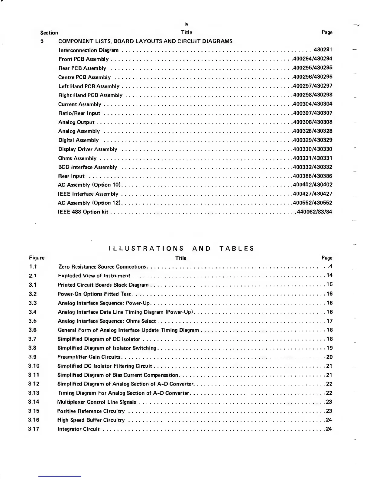
5 COMPONENT LISTS, BOARD LAYOUTS
AND CIRCUIT
DIAGRAMS
Interconnection Diagram
430291
Front PCB Assembly
400294/430294
Rear PCB Assembly
400295/430295
Centre
PCB Assembly
400296/430296
Left Hand PCB Assembly
400297/430297
Right Hand
PCB Assembly
400298/430298
Current Assembly
400304/430304
Ratio/Rear Input
400307/430307
Analog
Output
400308/430308
Analog Assembly
400328/430328
Digital
Assembly
400329/430329
Display Driver Assembly 400330/430330
Ohms Assembly
400331/430331
BCD Interface
Assembly
400332/430332
Rear Input 400386/430386
AC
Assembly (Option
10)
400402/430402
IEEE Interface Assembly
400427/430427
AC
Assembly (Option 12) 400552/430552
IEEE 488 Option kit 440082/83/84
ILLUSTRATIONS AND TABLES
Figure
Title
Page
1.1
Zero Resistance Source Connections
4
2.1 Exploded View
of
Instrument
14
3.1
Printed
Circuit Boards Block
Diagram
15
3.2 Power-On Options Fitted Test
16
3.3 Analog Interface Sequence;
Power-Up
16
3.4
Analog
Interface
Data Line Timing
Diagram (Power-Up)
16
3.5 Analog Interface Sequence: Ohms Select
17
3.6 General Form
of Analog Interface Update
Timing Diagram
18
3.7 Simplified Diagram
of DC
Isolator
18
3.8 Simplified Diagram
of Isolator Switching
19
3.9 Preamplifier Gain
Circuits
20
3.10 Simplified
DC Isolator
Filtering
Circuit 21
3.11 Simplified Diagram of Bias
Current Compensation 21
3.12 Simplified Diagram of Analog Section of
A-D
Converter
22
3.13 Timing Diagram For Analog
Section of A-D Converter 22
3.14 Multiplexer
Control Line Signals 23
3.15 Positive Reference
Circuitry
23
3.16 High
Speed
Buffer
Circuitry
24
3.17 Integrator
Circuit
24
 Loading...