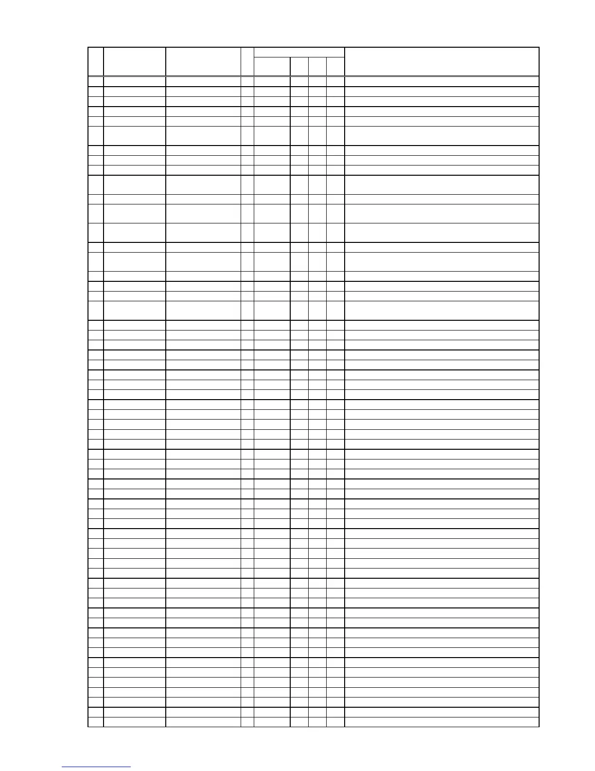
77
Pin
No
Port Name Port Name I/O
Status
Note
Pull-up/
down
init. stby Act.
20 TXD0 USB_TX/UPDATE TX O L L - send command to bolero IC
21 RXD0 USB_RX/UPDATE RX I - - - receive data from bolero IC
22 PE2 SP_ON O L L H speaker on/off control (AMP B'D Q710-E)
23 TXD1 DAB_TX O L L - send command to DAB Module
24 RXD1 DAB_RX I - - - receive data from DAB Module
25 PE6 DAC_FLT O - L -
DAC(PCM5100) Filter select : Normal latency(Low) / Low
latency(High)
26 PG0 DAB_DAO_TU_SDA I/O Pull-up L L H/L DAB Module I2C Data
27 PG1 DAB_CLK_TU_CLK O Pull-up L L H/L DAB Module I2C Clock
28 PG2 DAC_FMT O - L - Audio format selection : I2S(Low) / Left justied(High)
29 PB3 DAC_DEMP O - L -
DAC(PCM5100) De-emphasis control for 44.1kHz sampling
rate : Off(low) / On(High)
30 BOOT single boot mode I Pull-up - H L update mode select
31 PH1/TB0IN0 DAC_XSMT O - L -
DAC(PCM5100) Soft mute control : Softe mute(Low) / softe
un-mute(High)
32 PH2/TB1IN0 USB_OC O Pull-up
detect FLAG for NCP380 (Detect Over Current of USB
POWER)
33 TXD2 SP_OP O SP OPTIMIZE ON/OFF '(Initialize ON)
34 RXD2 DIR_IN I - - -
DIR(PCM9211(23)) IN(SPI data output DIR-OUT to MCU-
IN
35 PF2 F_V_CS O L L L function IC strobe (NJW1194)
36 PH3 F_V_CLK O L L - function IC clock (NJW1194)
37 PB4 F_V_DATA O L L - function IC data (NJW1194)
38 PI0 DIR_OUT O - L -
DIR(PCM9211(24)) Out(SPI data input) DIR-IN to MCU-
OUT
39 INT6 DIR_RERR I - - H DIR(PCM9211(1) Error detection output
40 PI1 DIR_CLK O - L - SPI clock input
41 PB5 DIR_CE O - L - SPI chip select
42 PI2 DIR_RST O - L L Reset input
43 PB6 BOL_RST O L L L Bolero (IC41) Reset
44 PF4 DAB_DAO_TU_SDA I/O tuner PLL IC data
45 PF5 DA_CLK_TU_SCL O tuner PLL IC clock
46 PF6 DAB_ON_TU_CE O tuner PLL IC chip select
47 PB7 TU_RST O tuner PLL IC reset
48 PI3 - O - - - OPEN
49 INT1 TU_INT I tuner PLL IC GPIO2
50 PK0 CD_BUS2 I - - - receive data from CD DSP (Oasis (64)pin OUT)
51 PK1 CD_BUS3 O L L - send command to CD DSP (Oasis (65)pin IN)
52 PI4 CD_BUCK O L L - communication clock with CD DSP
53 PI5 CD_CCE O L L - communication chip enable with CD DSP
54 PB0/TDO/SWV O Pull-up for DEBUG
55 PA0/TMS/SWDIO O Pull-up for DEBUG
56 PA1/TCK/SWCLK O Pull-down for DEBUG
57 TEST3 TEST pin, Set to OPEN.
58 PJ7 CD_DSP_RST O L L L CD DSP reset
59 PB1/TDI O Pull-up for DEBUG
60 PB2/TRST O Pull-up for DEBUG
61 PF3/RXIN1 - O OPEN
62 DVCC P Power supply pin
63 DVSS G GND pin
64 PA2 LED_RED O H H L TIMER ST LED(RED) Control ”L";ON
65 PA3 LED_GREEN O H H L Power LED (GRREN) Control "L";ON
66 PA4 VFD_RST O L L L vfd reset
67 PA5 VFD_DI O L L - vfd data
68 PA6 VFD_CS O L L L vfd chip select
69 PA7 VFD_CLK O L L - vfd clock
70 INT0 EX_INTERRUT I Pull-up - H L External Interrupt (For Key detection)
71 CVCC P Power supply pin
72 X2 oscillator(10MHz) high-speed oscillator(Output)
73 CVSS G GND pin
74 X1 oscillator(10MHz) high-speed oscillator(Input)
75 REGVSS GND pin G GND pin
76 REGVCC P Power supply pin
77 XT1 RTC oscillator(32.768KHz) low-speed oscillator(Input)
78 XT2 RTC oscillator(32.768KHz) low-speed oscillator(Output)
79 PI6/TB4IN0 - O OPEN
 Loading...