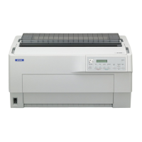
Epson DFX-9000 Revision B
Operating Principles Circuit operation 87
Printhead Control Circuit
The following shows a block diagram of the printhead control circuit.
Figure 2-33. Printhead Control Block Diagram
Printhead control
The printhead control circuitry includes the print data extraction section,
main excitation / flyback time selection section, print trigger generation
section, and the print timing control section. The timing control of the
printhead pins are based on:
1. The print data and density sent from the SoC ASIC, and
2. The 42 V voltage and CR encoder pulse input sent to the Mechanism
Control ASIC.
Figure 2-34. Printhead Control Block Diagram
SoC ASIC
ASIC
Printhead
ROM Board
Power Unit
Printhead
Control
Section
Flyback
absorption
circuit
Safety Check
Control
Section
Safety
Check
Detection
Section
D0-15HDIRQ A1-9
FB_01-36
PD01
PD02
FR2
FR1
FR9
GND
PD36
+42V
DIN00-15
PD01-09
PD11-19
PD21-29
PD31-39
FB01-09
FB11-19
FB21-29
FB31-39
HD_IRQ
42 V Voltage
CR Linear
Encoder_A
CR Linear
Encoder_B
Print Trigger
Generation
Section
Print Data
Extraction
Section
Print Timing
Control
Section
Main Excitation/
Flyback
Time Selection
Section
Print Trigger
DPISEL11-0
PRN_DIR
PD01-09 Print Data
PD11-19 Print Data
PD21-29 Print Data
PD31-39 Print Data
8BIT Main Excitation
Time for Front Head
8BIT FB Time
for Front Head
8BIT FB Time
for Rear Head
8BIT Main Excitation
Time for Rear Head

 Loading...


