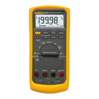
Digital Multimeter
Theory of Operation
13
Internal diodes on each pin of U1 clamp the voltage to a diode drop above or below the
power supply levels. Further, U1 power supplies are internally clamped together to
prevent overvoltage damage to circuits within U1. U1 pins 1 & 36 have the positive
clamp tied to the voltage at CPH (U1 pin 32), which is approximately 5 V above the
2.5-V power supply when the charge pump and current source in U1 are enabled. When
an overload voltage is present on the V/Ohms input jack with respect to the COMMON
input jack, clamp diodes in U1 conduct enough to drop the offending voltage on resistors
that handle the resulting overload current. Additional clamps, CR8, CR9, CR10 and
VR1, are used to keep currents from large overload voltages out of U1 pin 36 by safely
clamping the voltage at TP6 to approximately +8.9 V and -2.1 V with respect to
COMMON. Positive temperature coefficient thermistor, RT1, will aid the safe handling
of the overload by increasing in resistance and thereby reducing the overload current
being handled by these additional clamps. R1 is a high voltage resistor that drops the
overload voltage until RT1 can catch up.
During voltage overload conditions exceeding approximately ±2 kV at the V/Ohms input
jack, the open contacts of S1 need to have the voltage across them kept below the arc-
over level. RV1, RV2 & RV3 MOVs will conduct and limit the voltage at TP5 and TP11
to a magnitude of less than 2 kV unless TP5 is connected to TP6 by S1(1,2). The voltage
at TP6 will be held by clamps CR8, CR9, CR10 and VR1 as described above with RT1
and the high voltage resistor R1 safely dropping the overload voltage.
During voltage or current overload conditions at the mA/µA input jack with the mA/A or
µA Meter function selected, current shunts R4, R5 & R6 and the closed contacts of S1
are protected by F1 opening. CR1 & CR2 limit the voltage at the mA/µA input to
approximately ±2.1 V regardless of the Meter function selected, thereby protecting the
open or closed contacts of S1 (and the current shunts, if connected) while allowing time
for F1 to open.
During voltage or current overload conditions at the A input jack current shunt R6 is
protected by F2 opening.
C43 and R94, which are in parallel with Z1 (9.997 MΩ), are used in conjunction with
components in the signal conditioning circuit for frequency compensation. C3 reduces
input noise in the signal path. R100, R101 & R103 provide a current limited connection
to voltages that will minimize the leakage current of CR8, CR9 and CR10, which
combines with the input signal creating a temperature-dependent error in the reading.
Inductors L1, L2, L4 & L5 attenuate electromagnetic interference (EMI) and capacitive
coupled noise that is picked up by the input circuit and test leads that is passed to the
signal conditioning circuit.
The operation of R7, R10, R11, R48, C26, C31, CR5 and CR6 is described in
“Secondary Analog Circuits”.
Analog Signal Conditioning
U1 provides the switching that is necessary for range selection, the operational
amplifiers that are used for buffering and filtering, various current source values and
various voltage comparator functions, which are required to transform the input signal to
a representation that can be measured and quantified.
VAC
The V/Ohms input is connected, as described in Table 11, to DIV_A (U1 pin 3) and
routed by U1 internal switches to the inverting input of an internal operational amplifier.
The overall gain to ACAMP_O (U1 pin 22) is set by the total resistance to the inverting
input from the V/Ohms input, the selected range resistor in Z1, R105, R12 and R8. U1
works in conjunction with C43 & R94 to compensate the frequency response of this path.
The signal at ACAMP_O is, therefore, a scaled representation of the AC input signal

 Loading...