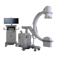
System Overview
2-67
GigE Camera use CCD sensor to acquire image on the output window of image intensifier. Following table shows
the key specification of CCD sensor.
Key Specification of CCD sensor of 5075006 and 5085003
Diagonal 11 mm (Type 2/3)
×
1024 (V) approx. 1.40M pixels
×
Key Specification of CCD sensor of 5491850,5491851 and 6491850
1000 (H) × 1000 (V) approx. 1.40M pixels
Camera System Control
In this structure, FPGA is central control unit of GigE Camera.
FPGA controls CCD driver electrical circuit to drive CCD sensor, then CCD sensor transfers the optical signal
into analog signal. VGA and 12-bit ADC convert analog signal to digital signal. FPGA buffers digital signal into
image buffer, then output per GigE Vision protocol.
FPGA can adjust the gain of image per receiving external gain control command from RS422 serial port.
FPGA provides two GPIO signal. One is Frame Sync output, the others is LIH input.
FPGA makes Frame Sync signal low for 5ms then high at every frame according 25FPS.
FPGA uses LIH signal to control transmitting of image as following: after 2 ms on the every falling edge of
Frame Sync, FPGA starts to check LIH. If LIH is continuous high for 10 ms, FPGA start to transmit image.
Otherwise, FPGA stops transmitting.
GigE Camera receives +12V DC as power input then converts different DC voltage to supply different circuits.
Interface
 Loading...