.
"I
, I
'\
, ",
.
..
,\,"
.)
"
"
"
"
Model '8730A & BSerieEr
"
:"'
'>:
'' ' " ,
'.',
"
I
TU RN
"OFF"
"TIME
I
TURN
i·
ON
"
'
'.
TIME
c:
I
"~l
"1'
" I ' ,I I
',I
. '
"
.
I
I
lay
-
t
\)
/
I
"
I
I
,
)
,
I
-
(
vee
I,
,
. ,
)
..
..
\
\.
+
!SV
I
I
, '
,
i
,
'.
,
,
"
I,
,
'1,
't
--..
-3V
.~
V-
i
I
I
••
-
•
,
, , ')1 I
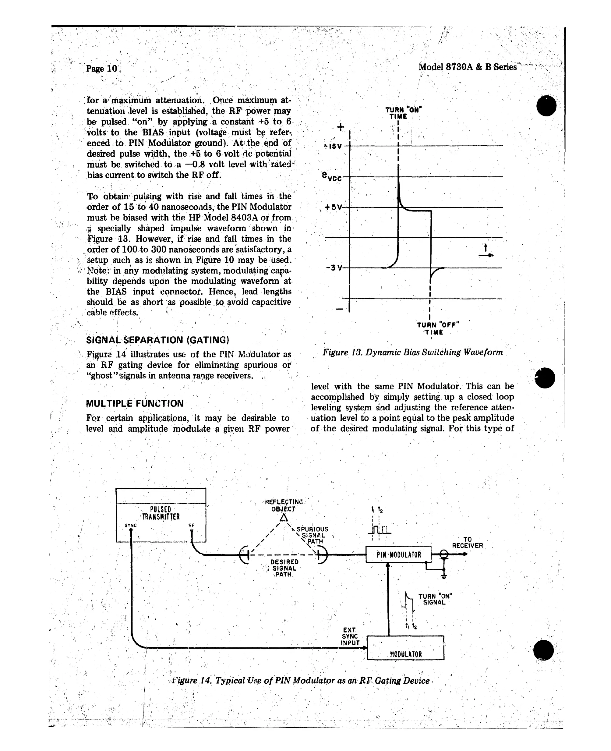
Figure 13. Dynamic
Bias
Switching
Waveform
..
'.
..":
','
,
,/
" , '
I ~
level with
the
.same PIN Modulator. This can
be'
, accomplished
by
simply
setting
up
a closed loop
leveling
system
~~d
adjusting
the
reference
atten-
uation
level
£0
a
point
equal
to
the
peak
amplitude
of
the
d~sir~d
modulating signal.
For
.this
type
of
.
I.'
•
,I:
';,
,
,J,'}
.'
_I:
\
I'
J"
•.
: ,
. /. "
.!/ ,,) /
'{I,
,:,·,':'l~",:i'\/ii1':'
".,r !
(.""
.'
'~',
\
" ';
'i'
,
"",",i
',:1
.·.·",.1,
I,'
,
..
"
.',
.'! '
"l
",,'
,:,','
,'I'
I I '
",
I •
~
I '.
" '
'I,'
"
". '
"
..".,
) '.,
MUL
TIPLEFUNCTION"
FQr"
c~rtain
applic;.ations, /it .may be desirable
to
level and amplitude.
modulate
a given RF power
"
,I
,I '
"
I,"
".:
Page
10
',:
"
'"
) I .'
'.
,
"...
',I'
. :
lor
a/maxinlum
attenuation.
',Once
.'
maximum
at-'.
',; "
" ;:
~
'. , : .1 "
'....
~,'
"
tenuation
.level is established,'
the
RFpowe,r
may
\, .,
'.
.
".
.
..
:be' pulsed
"on"
by applying .aconstant +5
to
,6
.,' '
'::volts'
to
the
"BIAS
input
(voltage'
,ntist'
b~
refer,; , :
".'
e~ce(r>to'PIN,Moduiator
ground).At~the·~~l(i
'o'f", .
. desired pulsewi,d,th,
the
,+5
to
6,
voltdepotential
'
must
beswitchedto.a
-0.8
volt levelwithratedv
.
'.
.
'.
.
.,
I
.bias
current
to
switch
the
RF
off.
' i :
SrGNALSEPARATION
(GATING)
, j • " 'I ,
;'\
Figure
14!
illustrates
u~,
of
the
rI~{
.Modulator as'
...'
an·
RF gating device
for
eliminetlng' spurious or'
" "gh'ost"'signals, in
antenna
range receivers.'
",
'r
,~
.
, .
. '
,>
',i
,'"
i'
,
.t
:'
To"
obtai~"p~lsing
with
rise'and
fall
'time~
in
~h~/
, , ) '.
order
of
15
'to
40
nanoseconds,
the
PIN Modulator
rnust be biased with
the'
HP
'Model
8403A
or
from, :
,",
,;!,,'
,I~
specially shaped' impulse
waveform'
sho~n"
in', '
",F~gure
-13.
However,
if
rise
,and
fall times in
the
, 'I. '
.order
of
100
to
300
nanoseconds
aresatisfactory
,a'
, " \
'setup
such as is shown
in
Figure
10
may be used.
;i:',
~l'Q'te:
in
any
modulating system,'modulating capa-
bility depends upon
the
modulating waveform'
at
the
BIAS
'input
·cQnnectQf. Hence,
lead,
lengths
. 1 . ,
I'
should-be as
short
.aspossibleto
avoid capacitive
,.cable effects. .i. ' .
" ,.
..
II,
I
,'
>,'
"
.',
"
J " .•
,
..
I •
}
I -,
, )
i'
\ .
. ,
, J
. ", .
I; ,
, '.
, ,
"
','I
".
,
,','i
, I' •
" ,
",
, ,
. , TO
,
RECEIVER.
.
PUt'MODULATOR
'1 t
2
,.' I
I I
,.nu.
::
i
",
.
DESIRED
:<',)
S'IGN1AL
,
,PATH.
'AEFlE(;T1
NG
I.'
,-
OBJECT· ,
~1"
.
/',
.
,/
I,"
SPU~'OUS
,/ .
.....
SI:~NP\L
'I
,/ "PATH
;I. .
."
,y
,/
""
'\\
~
__
........
_~,
'
__
l'~+-~"""~
RF
,
II"
I'
,
PULSED"
"TRANSMITTER
SYNC ' (
, '
"
'II
, ,
" '
f'.';
",'
.'."',
III
'j
"1
I
ii,
)
l';':,:,r
"
'-'
-
"
'e"
.
"
,.J
..
. " "
,
,1,'[
.' .
,
~
:1
'\.'
-,', t I .
I'
.j
•
) , i .
)
\'
t
l
\
,J
I I
,,:,'
"41
TURN"ON"
..
I,
SIGNAL
" I
I I
, I
t
l
'2
'1:)
',.1
"
, \
_.'
--~-
~~~-~~~._-----------
_.------'-------~.
__
.,-'
~
__
I"
_
..,
I
"
/
i .1
...
, .1
",
iJ
.:1
\.
) ,
'.
)
I
-
'.;.'
.
"
", .'.
~
!",
I
~,
fl I " '
,,'
.,"
•
',;'
':".
I
,I
J " )
,j,j?igure,14.
Typical'U~eof
PIN
~odu.latpr
as
an'R.-F'"
Gating
Device
'
, , '
.,
'I
.1
1
, I,"
··_·:'Y;'· T' ,
r
'\
:1
!
, I
./
..
"
'J""; :",1,
",i:.I
, , '
, .
i
,
\ '
. .:
.~
"
"I
'."
I
./
', '
'i "
 Loading...