Chapter 2. System Board Features
Chipset Control
The Intel Triton-VX chipset is the interface between the microprocessor and the following:
L2 cache controller
Memory subsystem
PCI bus
Bus master IDE connection
High performance PCI to ISA bridge
USB port
L2 Cache
The chipset supports an L2 cache that uses pipeline-burst, synchronous random access memory (SRAM).
L2 cache modules are removable and the base size module of 256 KB is upgradeable to 512 KB. In
addition to these sizes, a "cacheless" state with 0 KB of L2 cache is supported. Characteristics of each
L2 cache size are shown below.
The L2 cache is a look-aside, direct-mapped (one-way associativity) cache architecture. The L2 cache
operates in write-back mode, and by default, is implemented as unified cache (stores code and data). The
L2 cache supports the cache timings shown below.
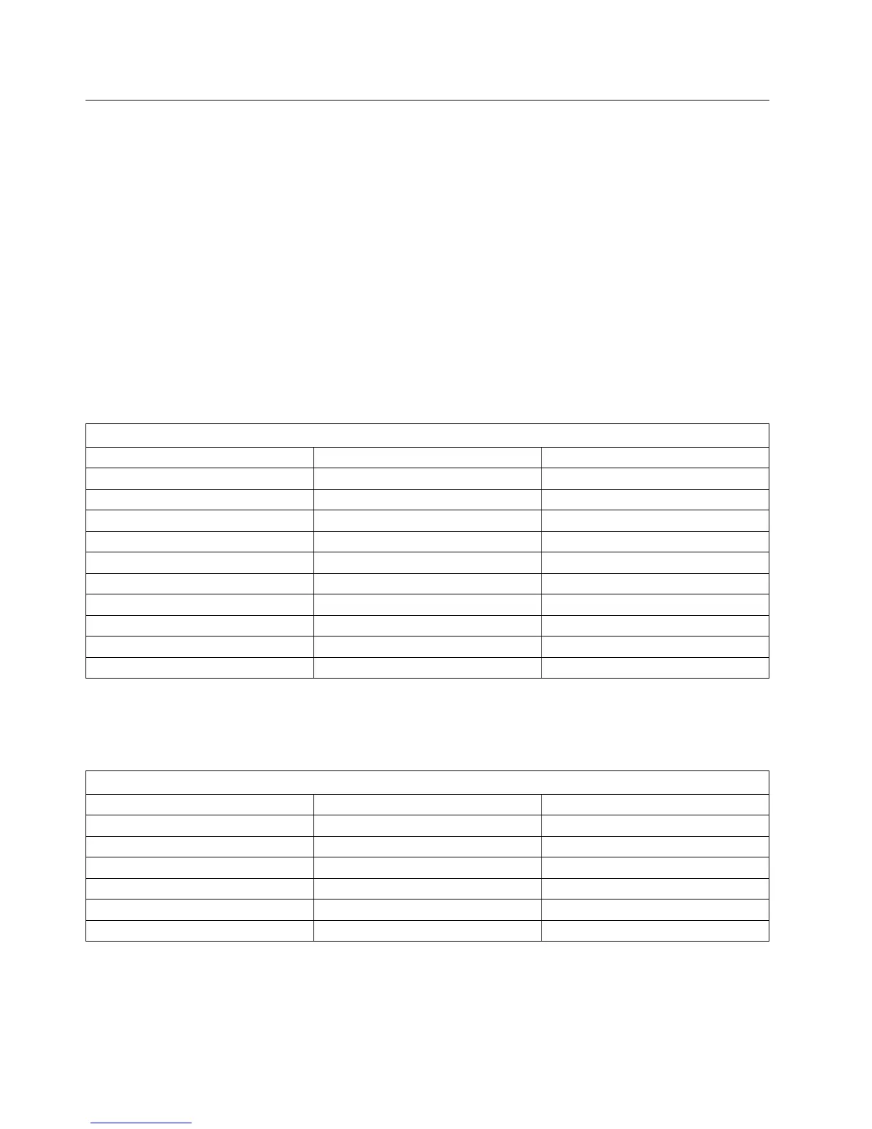
Figure 1. L2 Cache Characteristics
Cache Characteristics 256 KB L2 Cache 512 KB L2 Cache
Cacheable Memory 64 MB 64 MB
Line Size 32 bytes 32 bytes
SRAM Type 2 chips 32K x 32 4 chips 32K x 32
SRAM Voltage 3.3 V with 3.3 V output 3.3 V with 3.3 V output
SRAM Speed 8.5 ns 8.5 ns
Tag RAM Type 1 chip 8K x 8 2 chips 8K x 8 or 1 chip 16K x 8
Tag RAM Voltage 5 V 5 V
Tag RAM Speed 15 ns 15 ns
Tag RAM Tag Address A(25:18) A(25:19)
Tag RAM Set Address A(17:5) A(18:5)
Figure 2. L2 Cache Timings
Cycle 256 KB L2 (60/66 MHz) 512 KB L2 (60/66 MHz)
Single Read 3 3
Burst Read Hit 3-1-1-1 3-1-1-1
Burst Read Hit Pipelined 3-1-1-1-1-1-1-1 3-1-1-1-2-1-1-1
Single Write 3 3
Burst Write Hit 3-1-1-1 3-1-1-1
Write Miss NA NA
4 Technical Information Manual
 Loading...