RX-E112RSL/RX-E111RSL
1-16
1
2
3
4
5
6
7
8
9
18
17
16
15
14
13
12
11
10
P5
P6
P7
P8
Vss
P9
P10
p11
P12
VDD
P4
P3
P2
P1
CLR
STB
CLK
DATA
1~4
5
6~9
10
11
12
13
14
15
16~17
18
P5, P6, P7, P8
Vss
P9, P10, P11, P12
DATA
CLK
STB
CLR
P1
P2
P3, p4,
V
DD
O
-
O
O
I
I
I
O
O
O
-
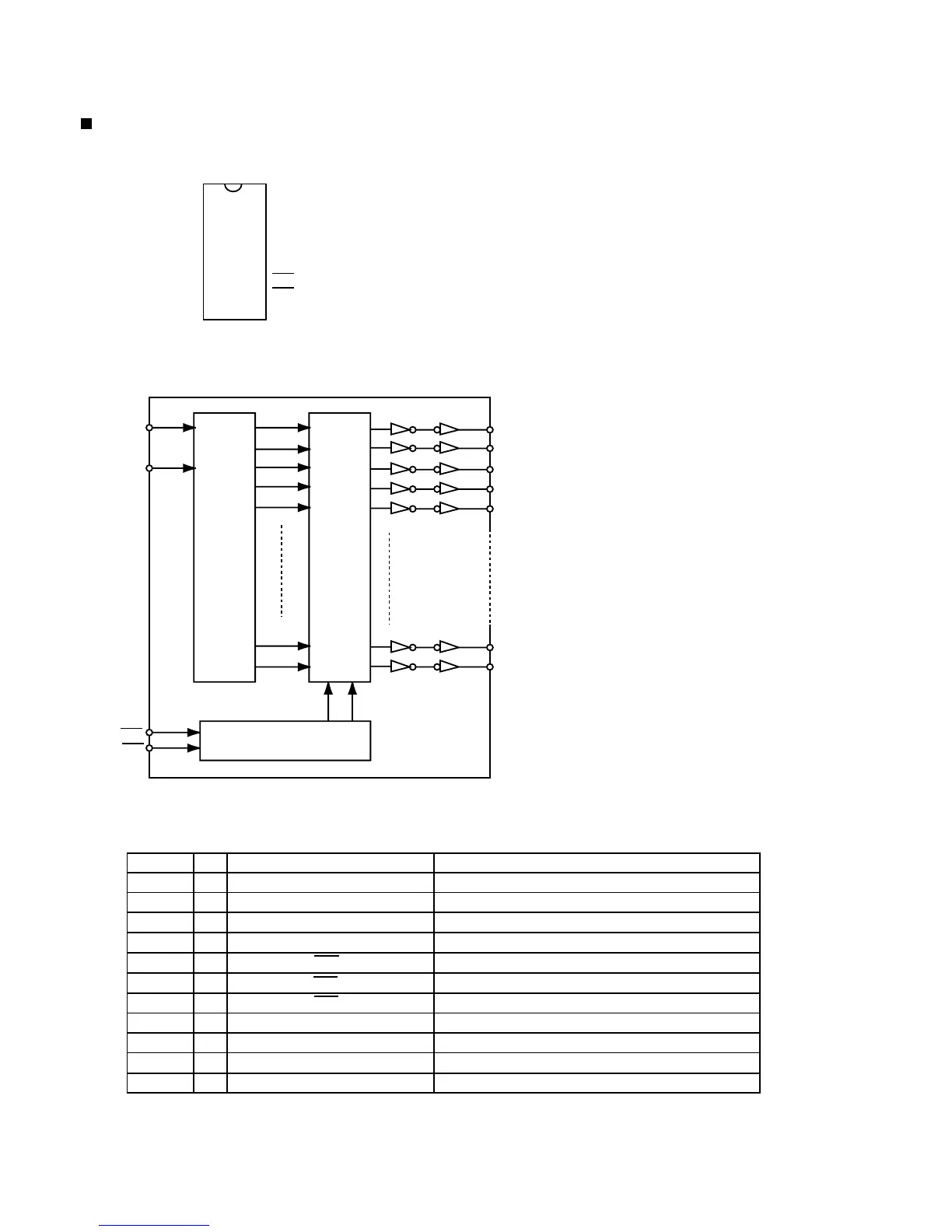
Parallel conversion data output terminal.
Connect to GND.
Parallel conversion data output terminal.
Serial data input terminal.
Clock signal input terminal.
Strobe signal input terminal.
Clear signal input terminal.
Parallel conversion data output terminal.
Parallel conversion data output terminal.
Parallel conversion data output terminal.
Power supply terminal.
PIN No.
I/O
Function
3.Pin function
1.Pin layout
Symbol
NJU3713 (IC402) : L.E.D. driver
DATA
CLK
STB
CLR
P1
P2
P3
P4
P5
P11
P12
Shift
resistor
Latch
circuit
Control Circuit
2.Block diagram