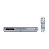
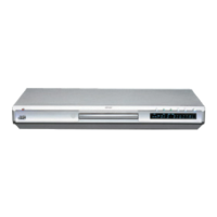
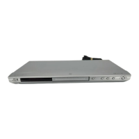
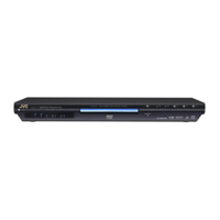
XV-N40BK,XV-N44SL
1-32 (No.A0040)
128 /HFMON - Non connect
129 SBAK - Non connect
130 HAGUP - Non connect
131 VI02 - Non connect
132 VSSio - Connect to ground
133 /DRVMUTE - Non connect
134 /SPMUTE - Non connect
135 VDD - Power supply terminal 1.8V
136~139 AD31~28 I/O Multiplexed address / data bus terminal
140 VDDio - Power supply terminal
141~144 AD27~24 I/O Multiplexed address / data bus terminal
145 PWE3 I/O Byte write enable for FLASH,EEPROM,SRAM or peripherals terminal
146 AD23 I/O Multiplexed address / data bus terminal
147 VSSio - Connect to ground
148~153 AD22~17 I/O Multiplexed address / data bus terminal
154 VDDio - Power supply terminal 3.3V
155 AD16 I/O Multiplexed address / data bus terminal
156 PWE2 I/O Byte write enable for FLASH,EEPROM,SRAM or peripherals terminal
157158 AD15,14 I/O Multiplexed address / data bus terminal
159 VDD - Power supply terminal 1.8V
160 SCLK O External bus clock used for programmable host peripherals
161 ACK I/O Programmable WAIT/ACK/RDY control
162 VSSio - Connect to ground
163~168 AD13~8 I/O Multiplexed address / data bus terminal
169 VDDio - Power supply terminal 3.3V
170 PWE1 I/O Byte write enable for FLASH,EEPROM,SRAM or peripherals terminal
171 VSS - Connect to ground
172~176 AD7~3 I/O Multiplexed address / data bus terminal
177 VSSio - Connect to ground
178~180 AD2~0 I/O Multiplexed address / data bus terminal
181 VDDio - Power supply terminal 3.3V
182 PWE0 I/O Byte write enable for FLASH,EEPROM,SRAM or peripherals terminal
183 ALE I/O Address latch enable
184~187 LA0~3 I/O Latched address 0~3
188 VSSio - Connect to ground
189 RD I/O Read terminal
190 LHLDA O Bus hold acknowledge in slave mode
191 LHLD I Bus hold request from external master in slave mode
192 VDD - Power supply terminal 1.8V
193 PCS0 O Peripheral chip select 0, generally used for enabling the program store ROM/FLASH
194195 XI01,02 I/O Programmable general purpose external input/output
196 VDDio - Power supply terminal 3.3V
197~200 XI03~06 I/O Programmable general purpose external input/output
201 VSS - Connect to ground
202 SODCCS I SODC Chip select
203 ADSCIRQ I Interrupt input
Pin No. Symbol I/O Description
 Loading...