NXR-700H
26
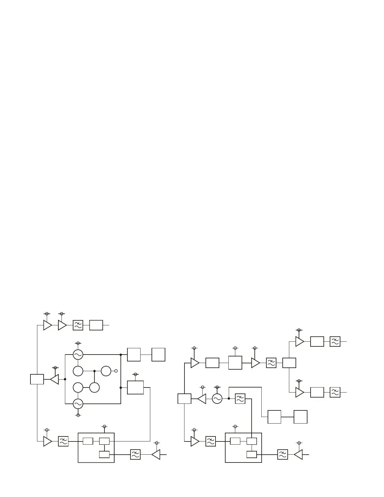
4-7. Receiver PLL circuits
The receiver unit (X55-309) has the 1st-PLL circuit for con-
trolling the VCO that generates the hetero signal to the fi rst
local oscillator, and the 2nd-PLL circuit for controlling the VCO
that generates the hetero signal to the second local oscillator.
The 1st-PLL circuit consists of the VCO (Q7 and Q8), the
Buffer amplifi er (Q17), the RF amplifi ers (Q16 and Q3), the
PLL-IC (IC5), the Active loop fi lters (Q2 and Q4) and the Band
switches (Q14, Q10, Q11 and Q59). The signal in the195.95
through under 209.95MHz band generated by VCO Q7 and
the 209.95 through 223.95MHz band generated by VCO Q8
is input to IC5 (pin5) via Q17 and Q16 as the Fin signal. The
6MHz reference signal generated by the DDS-IC (IC7) is input
to IC5 (pin8) via Q3. Two signals, Fin and REFin, are phase-
compared as the 100kHz comparison frequency by each
frequency divider. The VCO output with the frequency syn-
chronized is input to the 1st-Mixer as the fi rst local oscillator
Upper hetero signal approximately +17dBm via Q17, Q23,
and Q18. The control voltage is input to IC30 (ADC) pin16 via
IC6.
Meanwhile, the 2nd-PLL circuit consists of the VCO (Q24),
the Buffer amplifi er (Q33), the RF amplifi er (Q38, Q22), and
the PLL-IC (IC11). The 99.0MHz signal generated by Q24 is
input to IC11 (pin5) as the Fin signal via Q38. The 19.2MHz
Internal reference clock distributed by the transmitter unit
(X56-311) is input as the REFin signal to IC11 (pin8) via Q22.
Two signals, Fin and REFin, are phase-compared by each fre-
quency divider as the comparison frequency of 200kHz. The
VCO output with the frequency synchronized is input to IC9
(prescaler IC) pin2 via Q33 and Q21. The 49.5MHz signal is
frequency-divided into halves by IC9 and is excited by Q53
and distributed. One is input to IC12 (pin1) via Buffer ampli-
fi er_Q35. The other is input to IC13 (pin4) via Buffer ampli-
fi er_Q36. Both are input as approximately –16dBm for the
second local oscillator Lower hetero signal. The control volt-
age at this point is input to IC30 (ADC) pin10 via IC33.
Q17
1/N
1/R
PD
+5V
+5V
+9V
Q3
+5V
20
8
IC5
5
Fin
LPF
LPF
Q16
+9V
LPF
Q23
+9V
Q18
REFin
+9LV
+9LV
+9LV
+9LV
SW SW
Q10
SW SW
Q11
Q14
Q59
Q7
195.95~209.95MHz
Q8
209.95~223.95MHz
Div.
Active
LPF
IC6
16
IC30
ADC
IC9
1/2
IC33
10
IC30
ADC
Q2,4
Q33
1/N
1/R
PD
+5V
+5V
+9R
Q22
+5V
20
8
IC11
5
Fin
LPF
LPF
LPF
LPF
LPF
LPF
Q38
+5V
Q21
+5V+3V
Q53
+5VA
Q35
+5VD
Q36
REFin
Div.
Div.
ATT
ATT
ATT
ATT
Q24
99.0MHz
27
49.5MHz
Fig. 21 Receiver PLL circuits /
图 21 接收机 PLL 电路
CIRCUIT DESCRIPTION /
电路说明
4-7. 接收机 PLL 电路
接收机单元 ( X55-309) 具有第 1 PL L 电路,用于控制对第
一本地振荡器生成外差信号的 VCO ;以及第 2 PLL 电路,用于
控制对第二本地振荡器生成外差信号的 VCO。
第 1 PLL 电路由 VCO(Q7 和 Q8)、缓冲放大器 (Q17)、R F
放大器 (Q16 和 Q3)、PLL-IC(IC5)、有源环路滤波器 (Q2 和
Q4) 以及波段开关 (Q14、Q10、Q11 和 Q59) 组成。VCO Q7 生
成的 195.95 到 209.95M H z 以下频带中的信号,以及 VC O Q8
生成的 209.95 到 223.95M H z 频带中的信号,经 Q17 和 Q16 输
入 IC5( 针脚 5) 作为 Fin 信号。DDS-IC(IC7) 生成的 6MHz 基
准信号经 Q3 输入到 IC5( 针脚 8)。F in 和 REFin 两种信号由
各自的分频器进行相位对比,作为 100k H z 比较频率。频率同
步的 VC O 输出经 Q17、Q23 和 Q18 输入到第 1 混频器,作为
约 +17dBm 的第一本地上差信号。控制电压经 IC6 输入到 IC30
(ADC) 针脚 16。
同时,第 2 P L L 电路由 VC O ( Q24)、缓冲放大器 (Q33)、
R F 放大器 ( Q38、Q22) 和 PLL-IC(IC11) 组成。Q24 生成的
99.0M H z 信号经 Q38 输入到 IC11( 针脚 5),作为 Fi n 信号。
发射机单元分配的 19.2M H z 内部基准时钟作为 REFin信号经
Q22 输入到 IC11( 针脚 8)。Fin 和 REFin 两种信号由各自的分
频器进行相位对比,作为 200k H z 比较频率。频率同步的 VCO
输出经 Q33 和 Q21 输入到 IC9( 预计数器 IC) 针脚 2。49.5MHz
信号由 IC9 分频到一半,由 Q53 激励并进行分配。一个通过
缓冲放大器 Q35 输入到 I C12( 针脚 1)。另一个通过缓冲放大
器 Q36 输入到 IC13( 针脚 4)。二者被输入,作为第二本地
振荡器下差信号的约 -16dBm。此时控制电压经 IC33 输入到
IC30(ADC) 针脚 10。

 Loading...