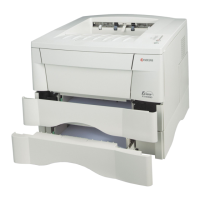
FS-6020
2-3-1
2-3-1 Power source PWB
D1
C7
F1
SW1
F2
Q1
D200
T1
C201
C202
C203
Zero cross
signal
detection circuit
(D8, D9, PC3)
Overcurrent/
overvoltage
detection circuit
Switching
control
circuit (IC1)
24 V DC rectification/
smoothing output circuit
D100
C101
C102
C103
5 V DC rectification/
smoothing output circuit
CR1
Fixing
heater
lamp
Fixing
heater
lamp
control
circuit
Power source PWB
AC
power
source
PC1
PC2
Noise
filter
circuit
(L1, L2)
TH1,TH2
Inrush current limit/rectification
smoothing circuit
+24V1
+24V2
+5V1
GND
GND
ZCROSS
HEATON
PC4
Pulse
Engine/high voltage PWB
Power
switch
SW2
Rear cover
interlock
switch
Figure 2-3-1 Power source PWB block diagram
The power source PWB consists of the switching regulator section that is the main part, other zero cross signal detection
circuit and fixing heater control circuit. The switching regulator circuit consists of the noise filter circuit, inrush current limit/
rectification circuit, switching control circuit, 5 V DC rectification/smoothing output circuit, 24 V DC rectification/smoothing
circuit and overcurrent/overvoltage detection circuit, and this circuit converts the AC power input to the 5 V DC and 24 V DC
power source by the switching operation and outputs it to the engine/high voltage PWB. The zero cross signal detection
circuit detects the 0 V point (zero cross) of the AC wave form and outputs to the engine/high voltage circuit, and the engine/
high voltage PWB outputs the fixing heater lamp ON signal (HEATON) to the fixing heater lamp control circuit based on the
timing of zero cross signal and controls the AC power loading to the fixing heater lamp.
 Loading...
