www.lairdtech.com/bluetooth
11
© Copyright 2018 Laird. All Rights Reserved
Americas: +1-800-492-2320
Europe: +44-1628-858-940
Hong Kong: +852 2923 0610
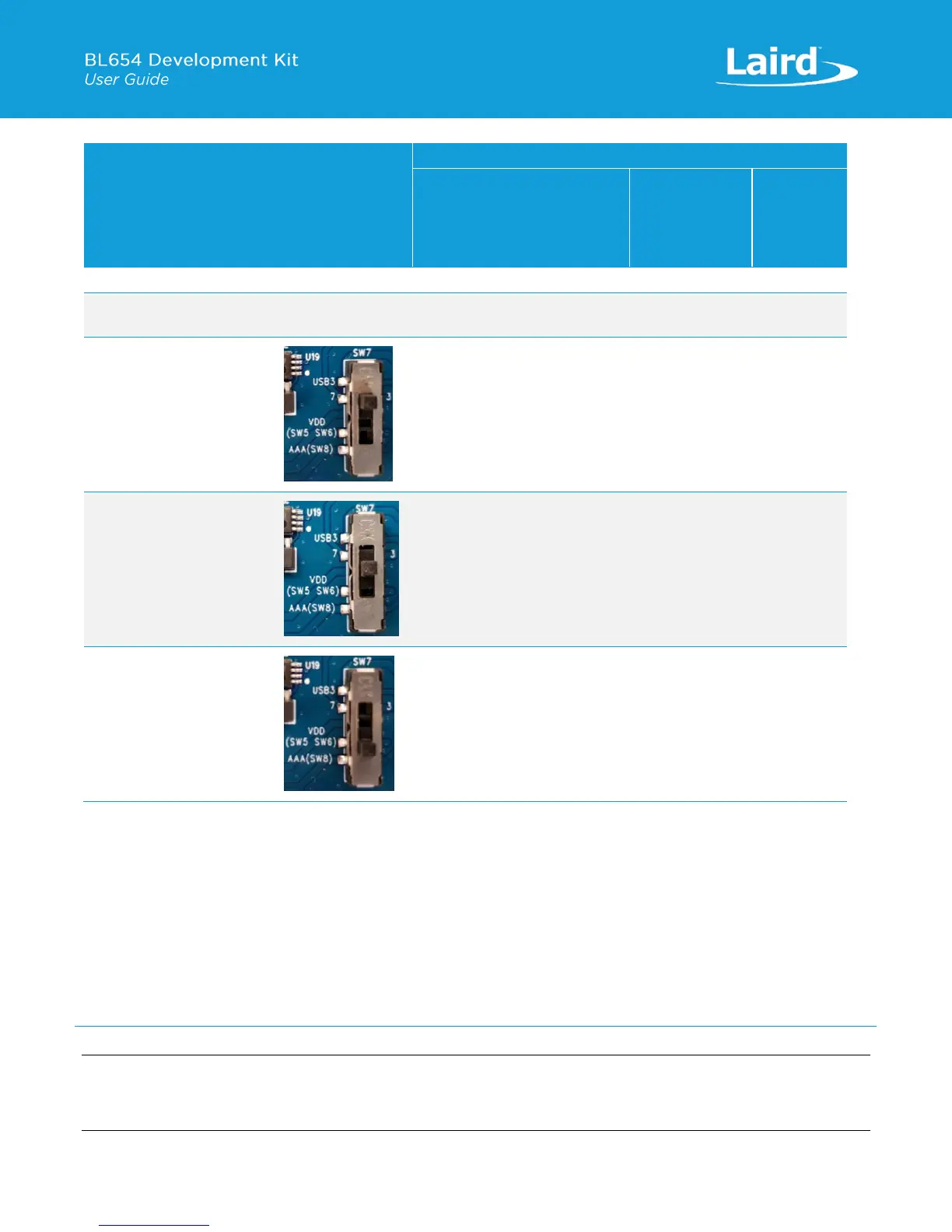
Table 1: Dev board power sources and switch positions
Selection Switch SW7 positions (silk screen)
Source
Voltage Operating mode
Dev Board Power Supply Switch Positions
SW5
Selects between
1.8V or 3.3V
SW8
Selects
between
2.5V or 4.5V
(3xAAA)
Connect
USB cable
into
USB3
Present selected voltage to the BL654 pin
SW7 Top position –
Silkscreen: USB3
(Source from USB3)
High Voltage Mode with
BL654 USB used (USB3)
SW7 Middle position –
Silkscreen: SW5 SW6
(Source from SW5, Note 2:
)
Normal Voltage Mode
Decided by SW5
(default SW5 on 3.3V position)
SW7 Bottom position –
Silkscreen: AAA (SW8)
(Source from SW8)
High Voltage Mode
Decided by
SW8
(default SW8 on
2.5V position)
Power Source and Switch Location Notes:
Note 1: No voltage is presented to VDD pin, as in High voltage mode, the VDD pin becomes an output voltage pin. It can
be used to supply external circuitry from the VDD pin. Before any current can be taken from the BL654 VDD pin,
this feature must be enabled in the BL654. Additionally, the VDD output voltage is configurable from 1.8V to
3.3V with possible settings of 1.8V, 2.1V, 2.4V, 2.7V, 3.0V, and 3.3V. The default voltage is 1.8V.
Note 2: When SW6 is set to position “coin-cell,” then the voltage selected with SW5 (default position 3V3) does not get
presented to the BL654. The CR2032 coin cell (in J34) voltage is not regulated but is fed directly to the BL654
module supply pin. Switch SW6 selects between the regulated 3V3V/1V8 and coin cell. The coin cell powers only
the BL654 module directly (on the development board); this is power domain VDD_nRF_SW through R46 0R.
Note: The development board for BL654 has on-board circuitry to allow access to BL654 SWD interface (via USB
connector USB2). Use USB2 only to power the development board when BL654 SWD interface is needed. Refer
to SWD Interface. When USB2 is used, USB1 does not need to be used for DC power.
 Loading...