– 2.2 –
2-1. Explanation of electrical components
2-1-1. Operations
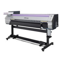
* The slider of the JV4 is provided with six heads with stagger arrangement, with 180 nozzles (at 180dpi
intervals) x 2 rows (2 colors) for each head.
* The ink in the ink chamber is discharged by vibrating the piezo-electric element of the head. The JV4
uses four different vibration waveform modes: the V1 (Variable1) mode which enables four gradations
(without L, M, and S) with 360 dpi resolution, the V2 (Variable2) mode which enables four gradations
with smaller dots with 720 dpi resolution, the N1 (Normal1) mode which enables high-speed two
gradations (1.0) with 360 dpi resolution, and the N2 (Normal2) mode which enables high-speed two
gradations with 720 dpi resolution.
However, note that the Normal waveform modes are not used when normal data is received from the
host PC. (Some Variable waveforms are represented in two gradations.)
Since the driving frequency (or the scanning speed of the head) depends on each waveform, Y-directional
position adjustment is required for each waveform.
* The HDC-4Head PCB is provided with two FPGAs (HDCs) which generate the driving signal (COM
waveform) to be applied to the piezo-electric element of one nozzle row for two heads, and the HDC-
2Head PCB is provided with one FPGA (HDC). The COM waveform is applied in synchronization with
the scale interval of each linear scale and, at the same time, the nozzle data is transferred to the head. Y-
directional position adjustment can be made in units of one dot or less by adjusting the timing of the
COM waveform for each nozzle row.
Since the ink discharge performance depends on each head, the COM waveform is corrected automatically
based on the head ID registered and the ambient temperature detected. (If the head ID is not registered
correctly, no ink may be discharged.)
* The main PCB is provided with the FPGA (PDC) in charge of image processing to which the 256MB
DSRAM picture memory (PRAM) is connected. As for the data output from the host PC, the command
is analyzed by the CPU and the image is transferred to the memory through high-speed DMA. Since the
PRAM has the ring memory configuration, head scanning is started when data for each scanning has
been stored. Since only an image with 180 dpi resolution can be formed into the X direction in each
scanning, the image with the target resolution is completed while making required amount of paper
feed.
* Stepping motors, sensors, and many other IO devices are connected to the JV4. Therefore, if all of them
are connected directly to the main PCB, it becomes difficult to handle wires and replace the PCB. To
avoid this, the number of signals has been reduced through serial signal transmission with the main PCB
using IO PCBs and ink sensor PCBs. This signal processing is performed by the FPGA (IOC) mounted
on the main PCB.
Scanning direction
180 dpi interval
Head nozzle arrangement
(viewed from rear side)
A#180
A#2
A#1
B#180
B#2
B#1
Paper feed
direction
Downloaded From ManualsPrinter.com Manuals
 Loading...