122
4 OPERATION CONTROL PROGRAMS
4.2 Device Descriptions
4.2 Device Descriptions
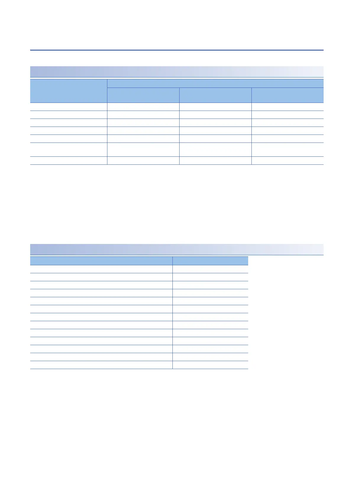
Word and bit device descriptions are shown below.
Word device descriptions
*1 Refer to the following for the setting range of usable device numbers(n).
MELSEC iQ-R Motion Controller Programming Manual (Common)
*2 = CPU number (CPU No.1: 0, CPU No.2: 1, CPU No.3: 2, CPU No.4: 3). A CPU number that exceeds the number of CPUs in Multiple
CPU system cannot be set.
*3 = 00h to FFh (Module I/O number 10h). The accessible range differs depending on the module. Refer to the manual of the module
used for details.
• For differentiation, the 32-bit floating-point type is ended by L and the 64-bit floating-point type by F (":F" for the link
register).
• For the 32-bit integer type and 64-bit floating-point type, specify the device number with an even number. (It cannot be set
as an odd number.)
Bit device descriptions
*1 Refer to the following for the setting range of usable device numbers(n).
MELSEC iQ-R Motion controller Programming Manual (Common)
*2 "m" indicates a word device bit specification (bit number: 0 to F).
*3 = CPU number (CPU No.1: 0, CPU No.2: 1, CPU No.3: 2, CPU No.4: 3).
A CPU number that exceeds the number of CPUs in Multiple CPU system cannot be set.
*4 = 00h to FFh (Module I/O number 10h).
The accessible range differs depending on the module. Refer to the manual of the module used for details.
Device name Device descriptions
*1
16-bit integer type 32-bit integer type
("n" is even No.)
64-bit floating-point type
("n" is even No.)
Data register Dn DnL DnF
Link register Wn WnL Wn:F
Special register SDn SDnL SDnF
Motion register #n #nL #nF
CPU buffer memory access device U3E\Gn
*2
U3E\GnL
*2
U3E\GnF
*2
CPU buffer memory access device
(fixed scan communication area)
U3E\HGn
*2
U3E\HGnL
*2
U3E\HGnF
*2
Module access device U\Gn
*3
U\GnL
*3
U\GnF
*3
Device name Device description
*1
Input relay Xn
Output relay Yn
Internal relay Mn
Link relay Bn
Annunciator Fn
Data register Dn.m
*2
Link register Wn.m
*2
Motion register #n.m
*2
Special relay SMn
Special register SDn.m
*2
CPU buffer memory access device U3E\Gn.m
*2*3
CPU buffer memory access device(fixed scan communication area) U3E\HGn.m
*2*3
Module access device U\Gn.m
*3*4
 Loading...