Pin Assignments
http://www.motorola.com/computer/literature B-3
B
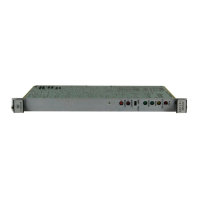
VMEbus Connector – P2
Row B of the P2 connector provides power to the MVME240x, the upper
eight VMEbus lines, and additional 16 VMEbus data lines as specified by
the VMEbus specification
. Rows A, C, Z, and D of the P2 connector
provide power and interface signals to a transition module, when one is
used. The pin assignments are as follows:
25 Not Used VA6 VIRQ6∗ VA13 Not Used 25
26 GND VA5 VIRQ5∗ VA12 Not Used 26
27 Not Used VA4 VIRQ4∗ VA11 Not Used 27
28 GND VA3 VIRQ3∗ VA10 Not Used 28
29 Not Used VA2 VIRQ2∗ VA9 Not Used 29
30 GND VA1 VIRQ1∗ VA8 Not Used 30
31 Not Used –12V +5VSTDBY +12V GND 31
32 GND +5V +5V +5V Not Used 32
Table B-2. P2 Connector Pin Assignment
ROW Z ROW A ROW
B
ROW C ROW D
1 PMC2_2 (J24-2) PMC1_2 (J14-2) +5V PMC1_1 (J14-1) PMC2_1 (J24-1) 1
2 GND PMC1_4 (J14-4) GND PMC1_3 (J14-3) PMC2_3 (J24-3) 2
3 PMC2_5 (J24-5) PMC1_6 (J14-6) RETRY# PMC1_5 (J14-5) PMC2_4 (J24-4) 3
4 GND PMC1_8 (J14-8) VA24 PMC1_7 (J14-7) PMC2_6 (J24-6) 4
5 PMC2_8 (J24-8) PMC1_10 (J14-10) VA25 PMC1_9 (J14-9) PMC2_7 (J24-7) 5
6 GND PMC1_12 (J14-12) VA26 PMC1_11 (J14-11) PMC2_9 (J24-9) 6
7 PMC2_11 (J24-11) PMC1_14 (J14-14) VA27 PMC1_13 (J14-13) PMC2_10 (J24-10) 7
8 GND PMC1_16 (J14-16) VA28 PMC1_15 (J14-15) PMC2_12 (J24-12) 8
9 PMC2_14 (J24-14) PMC1_18 (J14-18) VA29 PMC1_17 (J14-17) PMC2_13 (J24-13) 9
10 GND PMC1_20 (J14-20) VA30 PMC1_19 (J14-19) PMC2_15 (J24-15) 10
11 PMC2_17 (J24-17) PMC1_22 (J14-22) VA31 PMC1_21 (J14-21) PMC2_16 (J24-16) 11
12 GND PMC1_24 (J14-24) GND PMC1_23 (J14-23) PMC2_18 (J24-18) 12
Table B-1. P1 VMEbus Connector Pin Assignments (Continued)
 Loading...