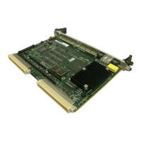
MVME2400 Base Board Preparation
http://www.motorola.com/computer/literature 1-9
1
Flash Bank Selection (J8)
Bank B consists of 1MB of 8-bit Flash memory in two 32-pin PLCC 8-bit
sockets.
Bank A consists of four 16-bit devices that are populated with 16Mbit
Flash devices (8MB). A jumper header, J8, associated with the first set of
four Flash devices provides a total of 64KB of hardware-protected boot
block. Only 32-bit writes are supported for this bank of Flash. The address
of the reset vector is jumper-selectable. A jumper must be installed either
between J8 pins 1 and 2 for Bank A factory configuration, or between J8
pins 2 and 3 for Bank B. When the jumper is installed, the SMC (System
Memory Controller) of the Hawk ASIC maps 0xFFF00100 to the Bank B
sockets.
System Controller Selection (J9)
The MVME240x is factory-configured in automatic system controller
mode; that is, a jumper is installed across pins 2 and 3 of header J9. This
means that the MVME240x determines if it is system controller at system
power-up or reset by its position on the bus; if it is in slot 1 on the VME
system, it configures itself as the system controller.
Remove the jumper from J9 if you intend to operate the MVME240x as
system controller in all cases.
Install the jumper across pins 1 and 2 if the MVME240x will not to operate
as system controller under any circumstances.
1
2
3
J8
Bank A (factory configuration)
1
2
3
J8
Bank B

 Loading...