Block Diagram
http://www.motorola.com/computer/literature 3-5
3
MPC750 Processor
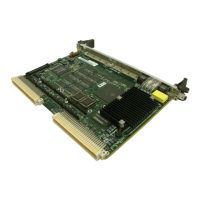
The MVME240x can be ordered with a PowerPC 750 processor chip with
32MB to 512MB of ECC SDRAM, and up to 9MB of Flash memory.
The PowerPC 750 is a 64-bit processor with 32KB on-chip caches (32KB
data cache and 32KB instruction cache).
The PHB bridge controller portion of the Hawk ASIC provides the bridge
between the PowerPC microprocessor bus and the PCI local bus.
Electrically, the Hawk is a 64-bit PCI connection. Four programmable map
decoders in each direction provide flexible addressing between the
PowerPC microprocessor bus and the PCI local bus.
The power requirements for the MVME240x are shown in Table 3-2.
L2 Cache
The MVME2400 SBC utilizes a back-door L2 cache structure via the
MPC750 processor chip. The MCP750’s L2 cache is implemented with an
onchip 2-way set-associative tag memory and external direct-mapped
synchronous SRAMs for data storage. The external SRAMs are accessed
through a dedicated 72-bit wide (64 bits of data and 8 bits of parity) L2
cache port. The board is populated with 1MB of L2 cache SRAMs. The L2
cache can operate in copyback or writethru modes and supports system
cache coherency through snooping. Parity generation and checking may be
disabled by programming the MCP750 accordingly. Refer to the
MVME2400 Programmer’s Reference Guide for additional information.
Table 3-2. Power Requirements
Configuration +5V Power +12V and –12V Power
233 or 350 MHz 750 3.3 A typical
4.0 A maximum
PMC-dependent
(Refer to Appendix A,
Specifications)

 Loading...