3-16 Computer Group Literature Center Web Site
Functional Description
3
low of a data tenure to the rising edge of the CLK that samples the
first TA_ low of the next data tenure.
3. The tB2 function reflects the number of CLK periods from the rising
edge of the CLK that samples the first TA_ low in a burst data tenure
to the rising edge of the CLK that samples the second TA_ low in
that data tenure.
4. The tB3 function reflects the number of CLK periods from the rising
edge of the CLK that samples the second TA_ low in a burst data
tenure to the rising edge of the CLK that samples the third TA_ low
in that data tenure.
5. The tB4 function reflects the number of CLK periods from the rising
edge of the CLK that samples the third TA_ low in a burst data
tenure to the rising edge of the CLK that samples the last TA_ low
in that data tenure.
Flash Memory
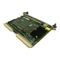
The MVME240x base board contains two banks of Flash memory. Bank
B consists of two 32-pin devices which can be populated with 1MB of
Flash memory. Only 8-bit writes are supported for this bank. Bank A has
four 16-bit Smart Voltage Flash SMT devices. With the 16Mbit Flash
devices, the Flash size is 8MB. A jumper header associated with the first
set of eight Flash devices provides a total of 128KB of hardware-protected
boot block. Only 32-bit writes are supported for this bank of Flash. There
will be a jumper to tell the Hawk chip where to fetch the reset vector. When
the jumper is installed, the Hawk chip maps 0xFFF00100 to these sockets
(Bank B).
The onboard monitor/debugger, PPCBug, resides in the Flash chips.
PPCBug provides functionality for:
❏ Booting the system
❏ Initializing after a reset
❏ Displaying and modifying configuration variables
❏ Running self-tests and diagnostics

 Loading...