Appendix B Timing Diagrams
M Series User Manual B-44 ni.com
Clock Generation Timing Diagrams
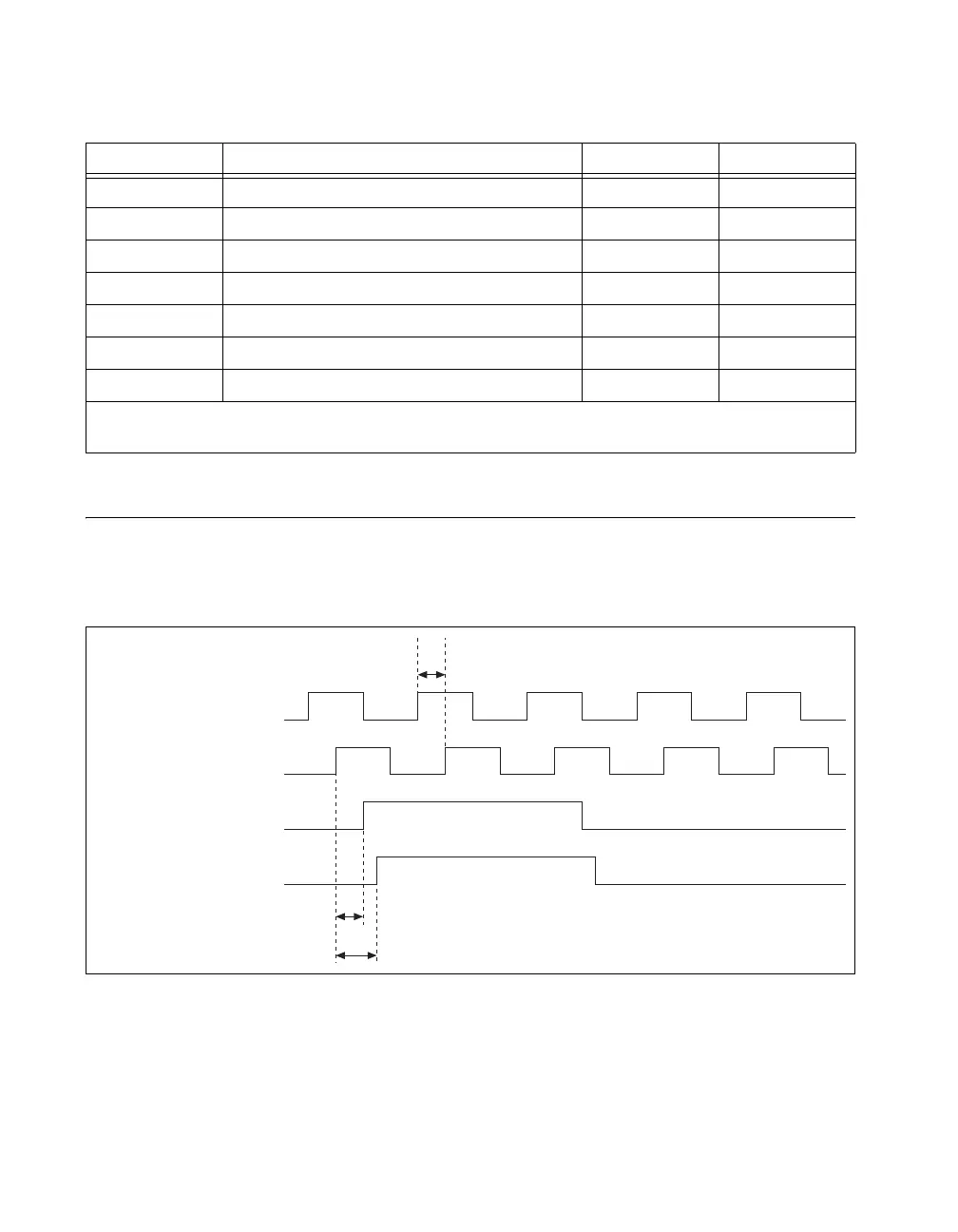
Table B-36 shows delays for generating different clocks, described in the
Clock Routing section of Chapter 9, Digital Routing and Clock Generation,
from the onboard 80 MHz oscillator.
Figure B-52. Generating Different Clocks from the Onboard 80 MHz Oscillator
Table B-35. Quadrature and Two Pulse Encoder Timing
Time Description Min (ns)
*
Max (ns)
t
14
Counter n A Period 50.0 —
t
15
Counter n A Pulse Width 25.0 —
t
16
Counter n B Period 50.0 —
t
17
Counter n B Pulse Width 25.0 —
t
18
Counter n Z Pulse Width 25.0 —
t
19
Delay from Counter n A to Counter n B 25.0 —
t
20
Delay from Counter n B to Counter n A 25.0 —
*
The times in this table are measured at the pin of the M Series device. For example, t
14
specifies the minimum period of a
signal driving a PFI, RTSI, or PXI_STAR pin when that signal is internally routed to Counter n A.
Onboard 80 MHz Oscillator
80 MHz Timebase
20 MHz Timebase
100 kHz Timebase
t
3
t
2
t
1
 Loading...