Table 4 Quantum Frequency Plan
Version Band Frequency Plan GMSK Power Class
EU GSM900 TX: 880-915MHz 4 (Max PCL5 = 33dBm)
RX: 925-960MHz
GSM1800 TX: 1710-1785MHz 1 (Max PCL0 = 30dBm)
RX: 1805-1880MHz
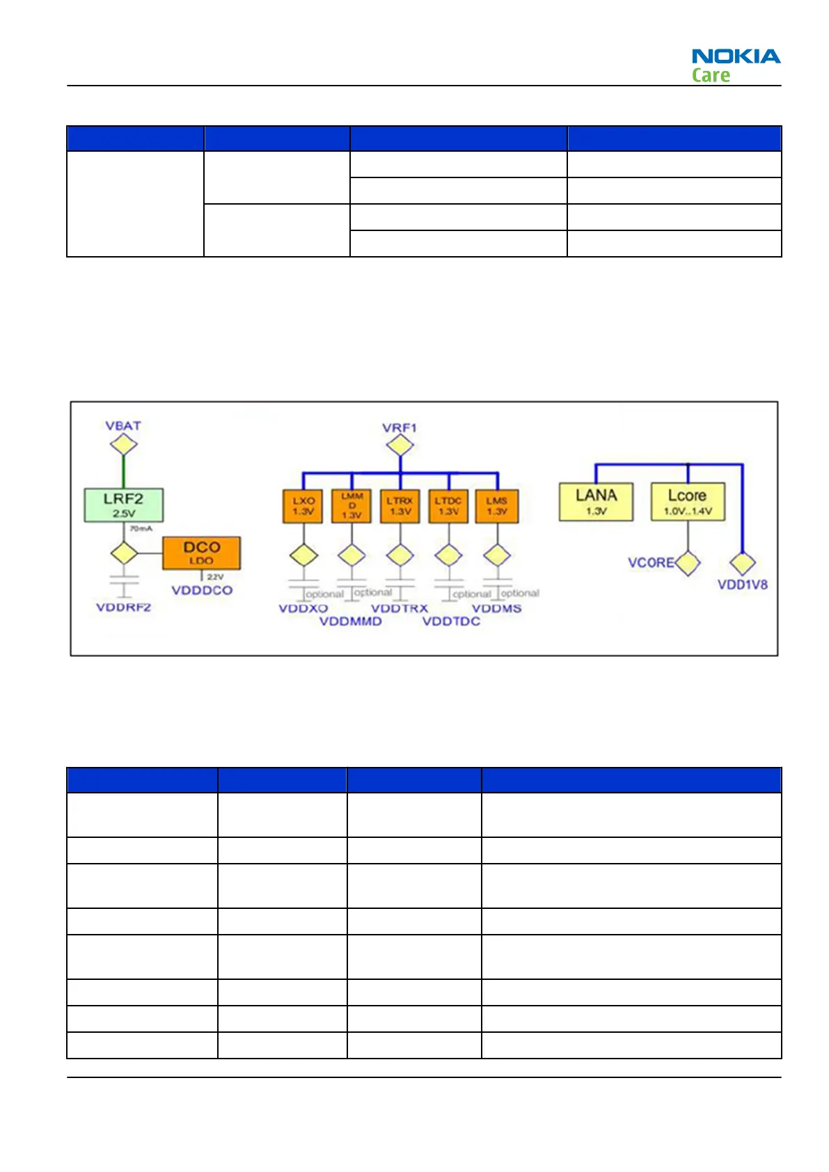
Regulators and power supply concept
In the X-GOLD213 IC, VRF1 and VDD1V8 are the regulated output voltages of the DCDC step down converter
and supply the RF, the digital core, and the analogue part. The remaining regulators are supplied by the
battery directly for increasing the efficiency.
The following figure shows the power concept of the X-GOLD213 IC RF sub-system.
Figure 72 Power concepts for X-GOLD213 RF sub-system
In the following table, the RF power supply names, IC ball numbers, description for use, and at which
components the supply voltage can be measured at are listed.
Table 5 Power supply voltages for the X-GOLD213 IC RF sub-system
Name Ball No. Test point Function
VBAT G14 C7134 3.6V typ. Battery voltage, supply voltage of
D2B LDO
VDDRF2 G13 C7106 2.5V D2B output voltage, part of RF supply
VRF1 H10 C7121 1.8V DCDC output voltage, supply of 1.3V
LDOs
VDDTRX B14 C7124 1.4V Transceiver supply
VDDTDC B12 C7131 1.3V VDD for Time to Digital Converter of
DPLL
VDDMS H13 C7123 1.3V Mixed signal supply
VDDXO E11 C7130 1.3V DCXO supply
VDDMMD A12 NONE 1.3V VDD for Multi Modulus Divider of DPLL
RM-704
System Module
Issue 1 COMPANY CONFIDENTIAL Page 5 – 25
Copyright © 2011 Nokia. All rights reserved.
 Loading...