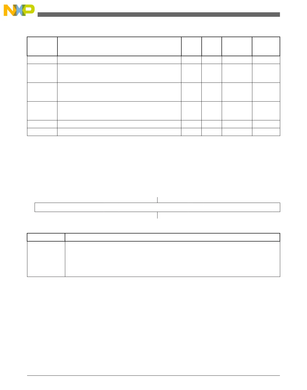
FGPIO memory map (continued)
Absolute
address
(hex)
Register name
Width
(in bits)
Access Reset value
Section/
page
F80F_F100 Port Data Output Register (FGPIOE_PDOR) 32 R/W 0000_0000h 41.3.1/780
F80F_F104 Port Set Output Register (FGPIOE_PSOR) 32
W
(always
reads 0)
0000_0000h 41.3.2/781
F80F_F108 Port Clear Output Register (FGPIOE_PCOR) 32
W
(always
reads 0)
0000_0000h 41.3.3/781
F80F_F10C Port Toggle Output Register (FGPIOE_PTOR) 32
W
(always
reads 0)
0000_0000h 41.3.4/782
F80F_F110 Port Data Input Register (FGPIOE_PDIR) 32 R 0000_0000h 41.3.5/782
F80F_F114 Port Data Direction Register (FGPIOE_PDDR) 32 R/W 0000_0000h 41.3.6/783
41.3.1 Port Data Output Register (FGPIOx_PDOR)
This register configures the logic levels that are driven on each general-purpose output
pins.
Address: Base address + 0h offset
Bit 31 30 29 28 27 26 25 24 23 22 21 20 19 18 17 16 15 14 13 12 11 10 9 8 7 6 5 4 3 2 1 0
R
PDO
W
Reset
0 0 0 0 0 0 0 0 0 0 0 0 0 0 0 0 0 0 0 0 0 0 0 0 0 0 0 0 0 0 0 0
FGPIOx_PDOR field descriptions
Field Description
31–0
PDO
Port Data Output
Unimplemented pins for a particular device read as zero.
0 Logic level 0 is driven on pin, provided pin is configured for general-purpose output.
1 Logic level 1 is driven on pin, provided pin is configured for general-purpose output.
FGPIO memory map and register definition
KL25 Sub-Family Reference Manual, Rev. 3, September 2012
780 Freescale Semiconductor, Inc.

 Loading...


