Timer Module (TIM16B8CV3)
MC9S12G Family Reference Manual Rev.1.27
NXP Semiconductors 755
NOTE
If the timer is not active (TEN = 0 in TSCR), there is no divide-by-64
because the 64 clock is generated by the timer prescaler.
For the description of PACLK please refer Figure 23-30.
If the pulse accumulator is disabled (PAEN = 0), the prescaler clock from the timer is always used as an
input clock to the timer counter. The change from one selected clock to the other happens immediately
after these bits are written.
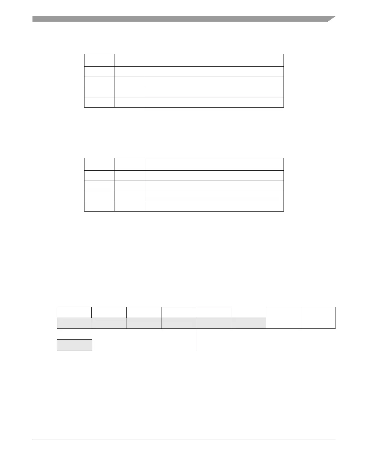
23.3.2.16 Pulse Accumulator Flag Register (PAFLG)
1
.
Read: Anytime
Write: Anytime
When the TFFCA bit in the TSCR register is set, any access to the PACNT register will clear all the flags
in the PAFLG register. Timer module or Pulse Accumulator must stay enabled (TEN=1 or PAEN=1) while
clearing these bits.
Table 23-19. Pin Action
PAMOD PEDGE Pin Action
0 0 Falling edge
0 1 Rising edge
1 0 Div. by 64 clock enabled with pin high level
1 1 Div. by 64 clock enabled with pin low level
Table 23-20. Timer Clock Selection
CLK1 CLK0 Timer Clock
0 0 Use timer prescaler clock as timer counter clock
0 1 Use PACLK as input to timer counter clock
1 0 Use PACLK/256 as timer counter clock frequency
1 1 Use PACLK/65536 as timer counter clock frequency
Module Base + 0x0021
76543210
R000000
PAOVF PAIF
W
Reset00000000
Unimplemented or Reserved
Figure 23-25. Pulse Accumulator Flag Register (PAFLG)

 Loading...


