FTFA memory map (continued)
Absolute
address
(hex)
Register name
Width
(in bits)
Access Reset value
Section/
page
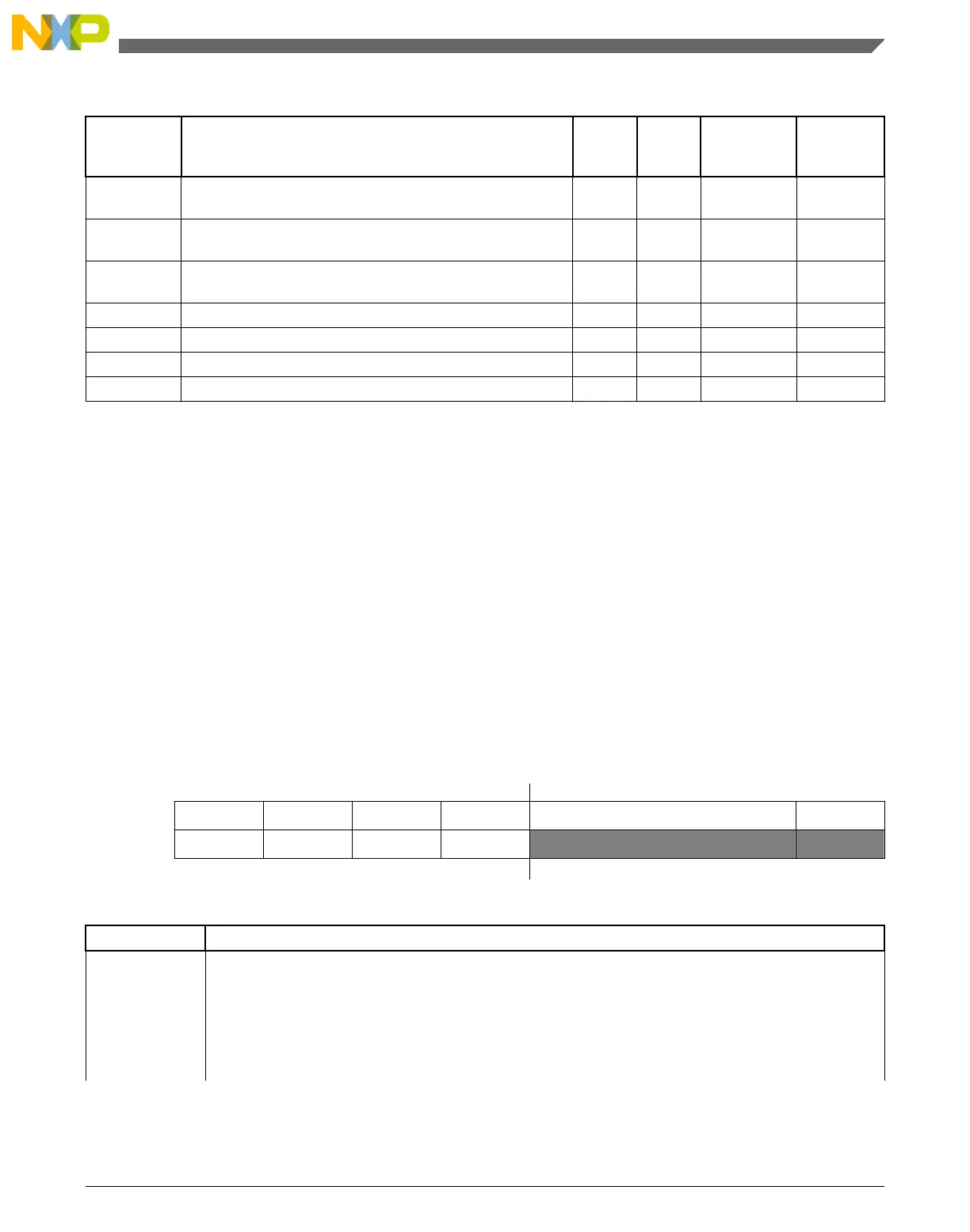
4002_000D
Flash Common Command Object Registers
(FTFA_FCCOBA)
8 R/W 00h 27.33.5/430
4002_000E
Flash Common Command Object Registers
(FTFA_FCCOB9)
8 R/W 00h 27.33.5/430
4002_000F
Flash Common Command Object Registers
(FTFA_FCCOB8)
8 R/W 00h 27.33.5/430
4002_0010 Program Flash Protection Registers (FTFA_FPROT3) 8 R/W Undefined 27.33.6/431
4002_0011 Program Flash Protection Registers (FTFA_FPROT2) 8 R/W Undefined 27.33.6/431
4002_0012 Program Flash Protection Registers (FTFA_FPROT1) 8 R/W Undefined 27.33.6/431
4002_0013 Program Flash Protection Registers (FTFA_FPROT0) 8 R/W Undefined 27.33.6/431
27.33.1 Flash Status Register (FTFA_FSTAT)
The FSTAT register reports the operational status of the flash memory module.
The CCIF, RDCOLERR, ACCERR, and FPVIOL bits are readable and writable. The
MGSTAT0 bit is read only. The unassigned bits read 0 and are not writable.
NOTE
When set, the Access Error (ACCERR) and Flash Protection
Violation (FPVIOL) bits in this register prevent the launch of
any more commands until the flag is cleared (by writing a one
to it).
Address: 4002_0000h base + 0h offset = 4002_0000h
Bit 7 6 5 4 3 2 1 0
Read CCIF RDCOLERR ACCERR FPVIOL 0 MGSTAT0
Write w1c
w1c
w1c w1c
Reset
0 0 0 0 0 0 0 0
FTFA_FSTAT field descriptions
Field Description
7
CCIF
Command Complete Interrupt Flag
The CCIF flag indicates that a flash command has completed. The CCIF flag is cleared by writing a 1 to
CCIF to launch a command, and CCIF stays low until command completion or command violation.
The CCIF bit is reset to 0 but is set to 1 by the memory controller at the end of the reset initialization
sequence. Depending on how quickly the read occurs after reset release, the user may or may not see the
0 hardware reset value.
Table continues on the next page...
Chapter 27 Flash Memory Module (FTFA)
KL25 Sub-Family Reference Manual, Rev. 3, September 2012
Freescale Semiconductor, Inc. 425
 Loading...


