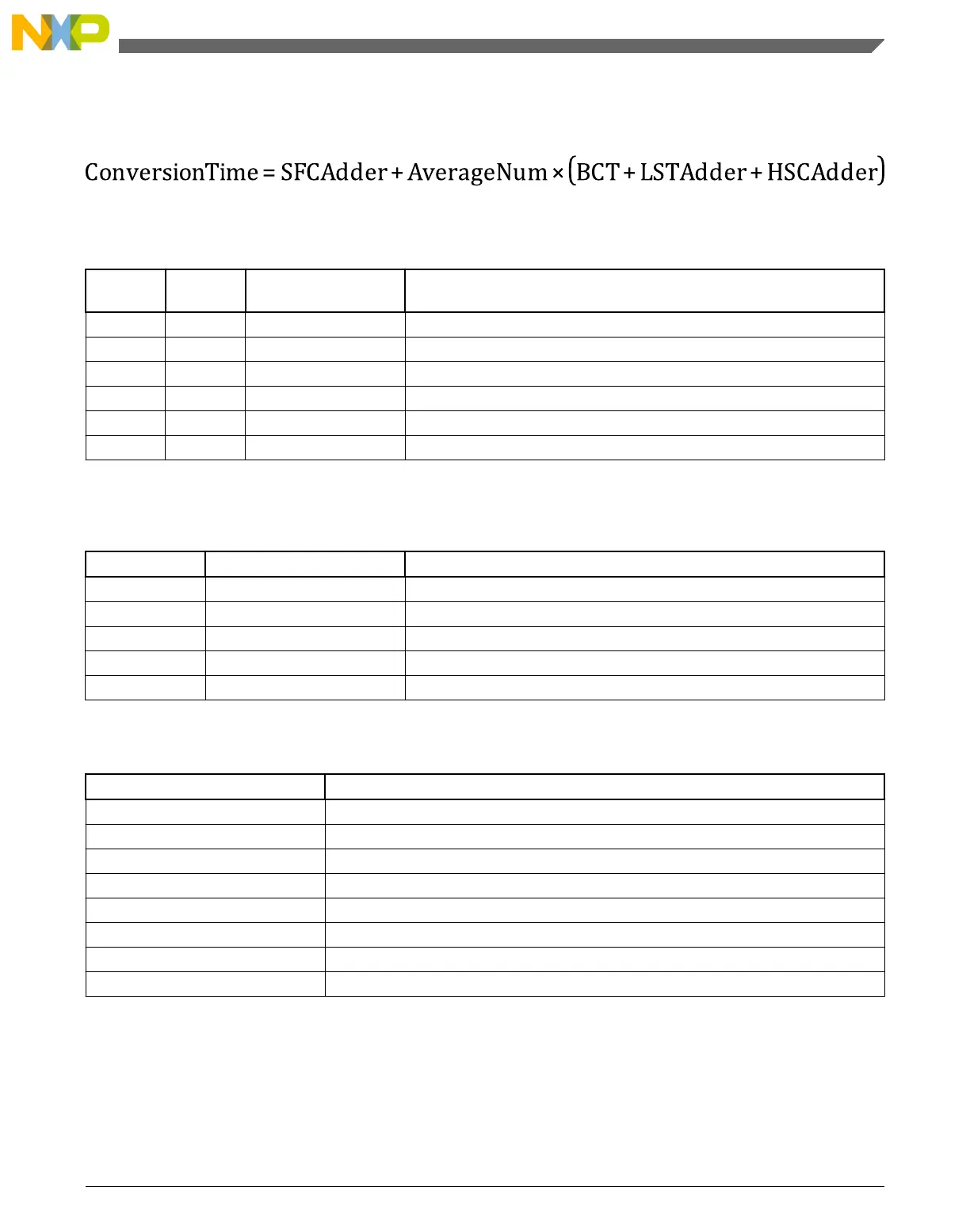
The maximum total conversion time for all configurations is summarized in the equation
below. See the following tables for the variables referenced in the equation.
Figure 28-62. Conversion time equation
Table 28-70. Single or first continuous time adder (SFCAdder)
CFG1[AD
LSMP]
CFG2[AD
ACKEN]
CFG1[ADICLK] Single or first continuous time adder (SFCAdder)
1 x 0x, 10 3 ADCK cycles + 5 bus clock cycles
1 1 11 3 ADCK cycles + 5 bus clock cycles
1
1 0 11 5 μs + 3 ADCK cycles + 5 bus clock cycles
0 x 0x, 10 5 ADCK cycles + 5 bus clock cycles
0 1 11 5 ADCK cycles + 5 bus clock cycles
1
0 0 11 5 μs + 5 ADCK cycles + 5 bus clock cycles
1. To achieve this time, CFG2[ADACKEN] must be 1 for at least 5 μs prior to the conversion is initiated.
Table 28-71. Average number factor (AverageNum)
SC3[AVGE] SC3[AVGS] Average number factor (AverageNum)
0 xx 1
1 00 4
1 01 8
1 10 16
1 11 32
Table 28-72. Base conversion time (BCT)
Mode Base conversion time (BCT)
8b single-ended 17 ADCK cycles
9b differential 27 ADCK cycles
10b single-ended 20 ADCK cycles
11b differential 30 ADCK cycles
12b single-ended 20 ADCK cycles
13b differential 30 ADCK cycles
16b single-ended 25 ADCK cycles
16b differential 34 ADCK cycles
Chapter 28 Analog-to-Digital Converter (ADC)
KL25 Sub-Family Reference Manual, Rev. 3, September 2012
Freescale Semiconductor, Inc. 489
 Loading...


