• Dedicated PMBus regulator for core power adjustable from 0.7 V to 1.3 V at 35
A
• USB
• Supports two USB 2.0 ports with integrated PHYs. Two type A ports with 5
V@1.5 A per port
• SDHC port that connects directly to card slot
• SPI
• One onboard 64 MB SPI flash
• Onboard support of SPI EEPROM, TDM SLAC control, and TDM riser card
control
• TDM interface through optional riser card, also support FXS/FXO on board
• I2C bus
• Devices connected: EEPROM, thermal monitor, VCore power controller
• Other IO
• Two serial ports
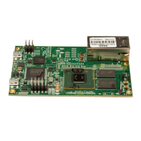
1.5 Block diagram
This section provides a high-level overview of the T1040 SoC and the T1040RDB board.
The figures below show the major functional units within the T1040 device and the
T1040RDB board.
(Peripheral access
management unit)
C
oreNet™ Coherency Manager
Security monitor
Power management
SD/eSDHC/eMMC
2x DUART
16b IFC
eSPI, 4x GPIO
32/64-bit
DDR3L/4
memory controller
Real-time
debug
Watchpoint
cross
trigger
Perf
Monitor
2 x USB2.0 w/PHY
4x I2C
Power Architecture
®
e5500
32 KB
D-Cache
32 KB
I-Cache
256 KB
backside
L2 cache
256 KB
platf
orm cache
Security fuse processor
DIU
Security
5.4
(XoR,
CRC)
P
attern
match
engine
2.2
Queue
Manager
Buf
fer
Manager
1G 1G 1G
Parse, classify,
distr
ibute
8-port
s
witch
1G 1G 1G 1G
1G 1G 1G 1G
2x DMA
PCl Express 2.0
PCI Express 2.0
PCI Express 2.0
PCI Express 2.0
SATA 2.0
SATA 2.0
TDM/HDLC
TDM/HDLC
QUICC
Engine
Trace
8-lane, 5 GHz SerDes
PAMU
Frame Manager
1G
Aurora
Figure 1-1. T1040 SoC block diagram
Block diagram
QorIQ T1040 Reference Design Board User Guide, Rev. 0, 06/2015
10 Freescale Semiconductor, Inc.
 Loading...


