NXP Semiconductors
S32K344
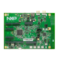
White Board
VDDIO VDD_HV_A
RST PTA5_MCU_RESETB
INT Interrupt input (PTG3)
FCCU1/FCCU2 FCCU_ERR0 / FCCU_ERR1 (PTF16/PTF14)
MUX-OUT ADC2_P7 input (PTE25)
Table 10. SBC and MCU connections...continued
8.2.2 SBC wakeup function
• Wakeup input by external key-on signal (0V to 12V transition on WAKE1).
– Push button SW7 on the board can generate such transitions.
• Wakeup input by LIN phy.
• Wakeup input by CAN phy or Ethernet phy.
8.2.3 SBC fail-safe outputs
SBC will pull FS0B and FS1B low when it detects certain failures, without MCU intervene.
• FS0B – disable high driver outputs (XS6500).
• FS1B – it’s left float and can be routed to customer desired circuit.
FS0B or FS1B assertion is indicated by LED D8 or LED D9 on the White Board. These
two signals can be released by special sequence of SPI commands. Refer to FS26
datasheet for details.
8.2.4 SBC debug mode
Jumper J5 needs to be closed and J87 to be open for the FS26 debug mode when
powering up. In this way the FS26 doesn’t need the watchdog refreshing from the MCU
by SPI.
Figure 12. SBC debug entry circuit
According to FS26 datasheet, the FS26 debug mode is entered if ~4V is detected on
FS26 DEBUG pin when FS26 is powered up. Then the FS26 starts to supply the MCU
when DEBUG pin back to GND. So a 4V pulse is seen during power-up on FS26 DEBUG
pin to enter debug mode.
UM11919 All information provided in this document is subject to legal disclaimers. © 2023 NXP B.V. All rights reserved.
User manual Rev. 1.0 — 11 April 2023
COMPANY PUBLIC 18 / 32
 Loading...