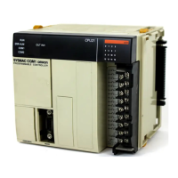
563
Specifications of Basic I/O Units Appendix A
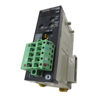
CJ1W-MD563 TTL I/O Unit (MIL Connector, 32 Inputs/32 Outputs)
Note The ON response time will be 20 µs maximum and OFF response time will be 400 µs maximum even if
the response times are set to 0 ms due to internal element delays.
Circuit Configuration
Output section (CN1) Input section (CN2)
Rated Voltage 5 V DC±10% Rated Input Voltage 5 V DC±10%
Operating Load Volt-
age Range
4.5 to 5.5 V DC Input Impedance 1.1 kΩ
Maximum Load Cur-
rent
35 mA/point, 560 mA/common,
1.12 A/Unit
Input Current Approx. 3.5 mA (at 5 V DC)
Leakage Current 0.1 mA max. ON Voltage 3.0 V DC min.
Residual Voltage 0.4 V max. OFF Voltage 1.0 V DC max.
ON Response Time 0.2 ms max. ON Response Time 8.0 ms max. (Can be set to between
0 and 32 in the PLC Setup.) (See
note.)
OFF Response Time 0.3 ms max. OFF Response Time 8.0 ms max. (Can be set to between
0 and 32 in the PLC Setup.) (See
note.)
No. of Circuits 32 points (16 points/common, 2 cir-
cuits)
No. of Circuits 32 points (16 points/common, 2 cir-
cuits)
Fuse None Number of Simulta-
neously ON Points
100% (16 points/common)
External Power Sup-
ply
5V DC±10%, 40 mA min. (1.2 mA ×
No. of ON points)
Insulation Resistance 20 MΩ between the external terminals and the GR terminal (at 100 V DC)
Dielectric Strength 1,000 V AC between the external terminals and the GR terminal for 1 minute at a leakage current
of 10 mA max.
Internal Current Con-
sumption
5 V DC 190 mA max.
Weight 110 g max.
Accessories None
IN00
IN15
COM2
IN00
IN15
COM3
COM2
COM3
1.1 kΩ
2.2 k
Ω
1000 pF
1.1 kΩ
2.2
Ω
1000 pF
OUT00
+V
OUT15
COM0
OUT00
+V
OUT15
COM1
COM0
COM1
5.6 k
Ω
5.6 k
Ω
CN1 (OUT)
CN2 (IN)
to
Indicator switch
Input indicator
to
Output indicator
Indicator switch
Internal circuits
Internal circuits
to
to
 Loading...