AND8344/D
www.onsemi.com
13
frequency for each half of the period. It is recommended to
keep power signals as short as possible in the PFC and the
STBY stages. This SMPS is designed on a single layer PCB
with several wire jumpers.
Results
To test efficiency and EMI please follow the steps detailed
in test procedure available on the ON Semiconductor web
site. The tests show that the demoboard meets all of the
requirements for a typical LCD TV. Additional
measurements are shown below for further information on
the operation of the design.
Thanks
ON Semiconductor thanks the companies:
Jepuls − http://www.jepuls.cn/En
Epcos − http://www.epcos.com
Koshin − http://www.koshin.com.hk
Pulse − http://www.pulseeng.com
Wurth − http://www.we−online.com
Coilcraft − http://www.coilcraft.com
for providing the samples used on this demoboard.
Conclusion
This demoboard shows only one of many possible
implementations of the NCP1392 resonant controller and is
not intended as final design for end customers. The main
goal of this document is to illustrate a typical application
where these controller would be used and illustrate some
functions that can be implemented with external
sub-circuits. Many options are included on the PCB, so it is
easy to update an application according to specific requests.
The following are are a series of scope plots that may be
helpful in understanding the operation of the SMPS under
different conditions.
References
[1] Data Sheet NCP1392B/D
[2] Data Sheet NCP1606B/D
[3] Data Sheet NCP1351/D
[4] Application Note AND8123/D
[5] Application Note AND8255/D
[6] Application Note AND8257/D
[7] Application Note AND8327/D
[8] Bo Yang − Topology Investigation for Front-End
DC−DC Power Conversion for Distributed Power
System
[9] M. B. Borage, S. R. Tiwari and S. Kotaiah − Design
Optimization for an LCL − Type Series Resonant
Converter
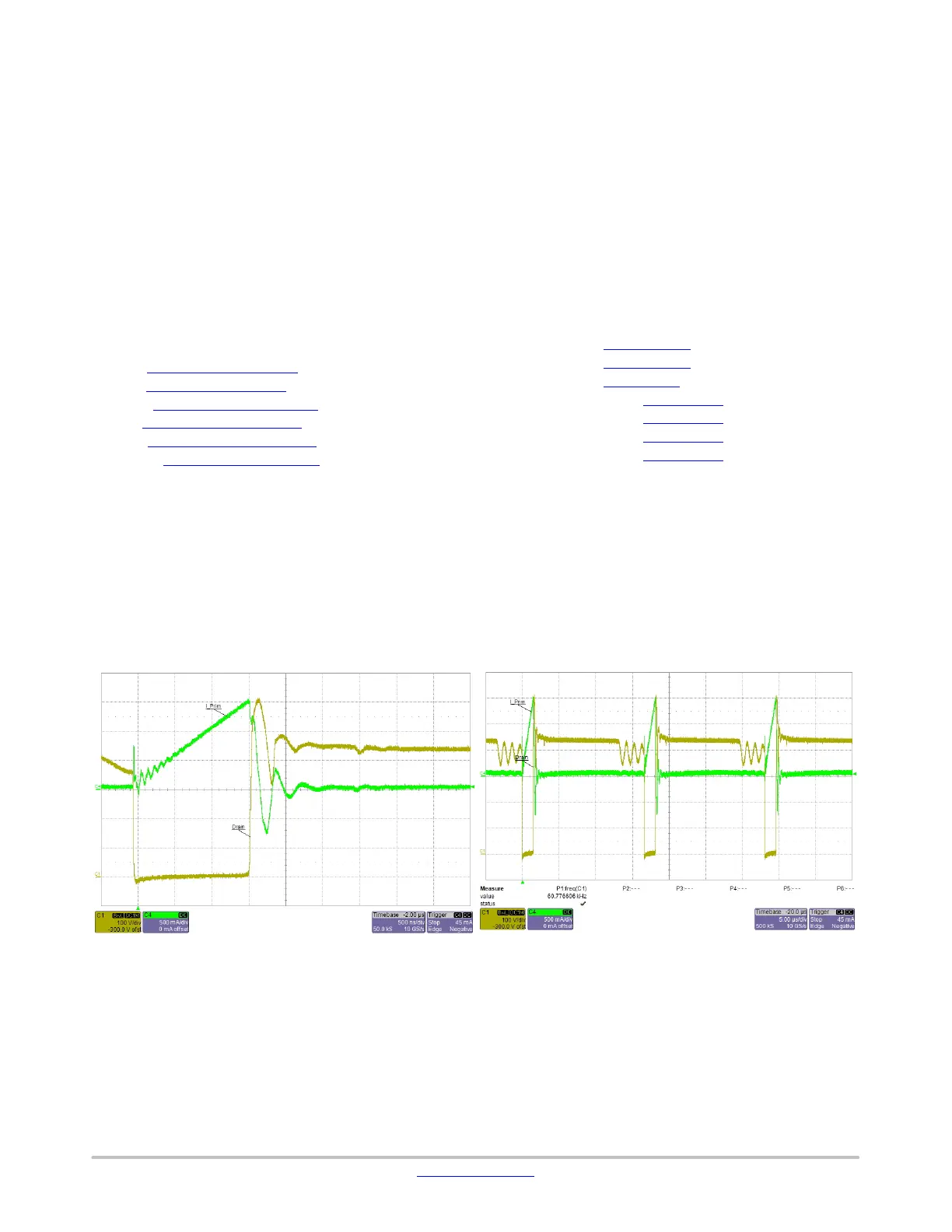
Figure 16. Detail of the drain current and
voltage of the STBY SMPS for 20 W load and
nominal V
bulk
. An 800 V MOSFET is used. The
max drain voltage for this figure is 600 V, so
the transistor is safe.
Figure 17. STBY primary current and drain
voltage for 20 W load, nominal V
bulk
. SMPS
operates at 60 kHz.
 Loading...