13 12 11 10 9 8 7 6 5 4 3 2 126
14 15 16 17 18 19 20 21 22 23 24 2527
SW +5V M
(TO MAIN C.B.A. P6201)
CAP VM (+16V)
CAP FG
GND (FG)
TL
CAP ET
CAP F/R
GND (M)
1
2
3
4
5
6
7
8
CNF PCI CT2 CT1 CST GND VG R IN F IN OUT2 L GND OUT1 VM2
EC PG+ PG- PG OUT PFG VCC COM VM M1 M2 RNF M3
LOWER
SATURATION
PREVENT
CIRCUIT
SOFT
SWITCH
STARTING
CONTROL
LOGIC
TSD
CONTROL
LOGIC
RRE-DRIVE
AMP AMP
MOTOR
DRIVE
PRE-DRIVE
MOTOR
DRIVE
SIGNAL
GENERATOR
SELECTOR
DIFFERENTIAL
AMP
DIFFERENTIAL
AMP
DIFFERENTIAL
AMP
PG/FG
COMPOSER
15
16
17
22
23
24
25
26
27
21
CAPSTAN
MOTOR
COILS
HALL
HALL
HALL
H3-
H3+
H1-
H1+
H2-
H2+
A1
A2
A3
VH+
MOTOR
DRIVE
DIFFERENTIAL
AMPLIFIRE
TORQUE
CONTROL
TL
AMP
EC
AMP
DEF
AMP
POSITION
SIGNAL
PROCESS
TORQUE
DIRECTION
SELECT
HALL
POWER
VM
TL
EC
ED/S
19
9
10
11
CAPSTAN
FG
HEAD
IC6201
CYLINDER/LOADING MOTOR DRIVE IC-DETAIL BLOCK DIAGRAM
CYLINDER SERVO
CAPSTAN MOTOR ASS'Y BLOCK DIAGRAM
CAPSTAN SERVO
CAPSTAN MOTOR DRIVE IC
NOTE:CAPSTAN MOTOR ASS'Y IS SUPPLIED AS A UNIT ONLY.
I/O CHART OF IC6001
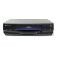
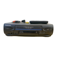
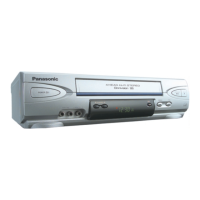
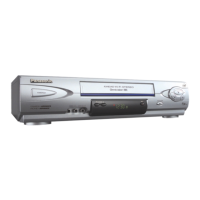
PV-V4524S/PV-V4624S/PV-V464S/PV-V4524S-K/PV-454S-K/PV-V4624S-K
I/O CHART OF IC6001
1 KEY 1 I KEY DATA 1
2 KEY 2 I KEY DATA 2
3 KEY 3 I KEY DATA 3
4 KEY 4 I KEY DATA 4
5 CYL REG SHORT L I REG12V short detection signal.
6 DTS AFC I Input terminal for "S-Curve" of Tuner AFC at channel selecting.
7 S PHOTO I Input terminal of the Tape End sensor detection.
*More than 2.6V: Black tape part. *Less than 2.4V: Trans. Tape part.
8 T PHOTO I Input terminal of the Tape Beginning sensor detection.
*More than 2.6V: Black tape part. *Less than 2.4V: Trans. Tape part.
9 TR ENV I Input terminal of the Video envelope signal.
10 MTS MODE I *STEREO + SAP: More than 2.6V *STEREO: 1.6V - 2.5V
*MONO + SAP: 0.6V - 1.5V *MONO: 0 - 0.5V
11 TL O Control terminal for the Capstan current limit.
12 NC O Low fix.
13 V L PLS O Output terminal for the Artificial V-sync.
14 IR DATA I Input terminal for the Remote Controller.
15 NC O Low fix.
16 NA PB SW ON L O Recording control signal for the Linear Audio.
17 NC O Low fix.
18 HSW O Video head switching signal
*L'/R = "High" *R'/L = "Low"
19 HF HSW O Head switching signal for Audio circuit.
20 D REC H O Video Delay Rec H
21 NC O Low fix.
22 DEFEAT H O Input/Output terminal for muting at channel selecting.
23 HIFI ADJ H O During Hifi Vco adjustment: "Low"
24 NC O Low fix.
25 NC O Low fix.
26 HIFI PB H I HiFi playback: "High" Normal playback: "Low"
27 NO S TAB L I SAFETY TAB DETECTION
*With SAFETY TAB: "Low" *Without SAFETY TAB: "High"
28 A MUTE H O Audio muting signal: High = ON
29 3CH Hiz/4CH L O CH3: Hiz CH4: L
30 POS 4 I MODE SW POSITION 4
31 POS 3 I MODE SW POSITION 3
32 POS 2 I MODE SW POSITION 2
33 POS 1 I MODE SW POSITION 1
34 RST L I RESET Terminal.
35 XC IN I (Not used)
36 XC OUT O (Not used)
37 DVDD - VCC (5V) for Digital port.
38 X IN I Main clock (12MHz) osc. input terminal.
39 X OUT O Main clock (12MHz) osc. output terminal.
40 DVSS - Digital GND for OSC circuit.
41 OSC IN3 I (Not used)
42 OSC OUT3 O (Not used)
43 SUB CLK ST L I 5V fix.
44 LC OSC IN I Input terminal of the LC Oscillation (For OSD dot clock)
45 LC OSC OUT I Output terminal of the LC Oscillation (For OSD dot clock)
46 NUB - Connected to the GND (Test terminal "B" in the factory).
47 4FSC LPF I OSC Filter connection terminal for Internal sync generator.
48 OSD FSC IN I Sub carrier (fsc) input terminal for sync generator.
49 VSS OSD - GND terminal for OSD circuit.
50 CV-IN I Input terminal for composite video signal.
Pin
No.
Signal Name I/O Explanation
51 BW H/COLOR L I (Not used)
52 CV OUT O Output terminal for composite video signal.
53 VDD OSD - Power supply terminal for OSD.
54 HLF I LPF connection terminal for slicer.
55 V HOLD I Capacitor connection terminal of the Reference voltage generator
circuit for the slicer.
56 CV IN I Composite video signal input terminal for the slicer.
57 NUA - Connected to the GND (Test terminal "A" in the factory).
58 SCAN2 O Scan pulse 2
59 SCAN1 O Scan pulse 1
60 KEY IN OPTION 4 I Option/Key input terminal 4
61 VCR H/TV L O TV: L VCR: H
62 KEY IN OPTION 2 I Option/Key input terminal 2
63 KEY IN OPTION 3 I Option/Key input terminal 3
64 KEY IN OPTION 1 I Option/Key input terminal 1
65 LOADING REV H O Loading motor control terminal.
66 PANE CS O LED serial chip selector
67 LOADING FWD H O Loading motor control terminal.
68 IC DATA OUT O Serial data output for LED.
69 IC DATA IN I Low fix.
70 IC DATA CLK O Serial clock output for LED.
71 IIC CLK O Serial communication terminal (IIC) for IC3001/FM audio IC/
EEPROM/TUNER.
72 IIC DAT I/O Serial communication terminal (IIC) for IC3001/FM audio IC/
EEPROM/TUNER.
73 750kHZ/ROM CORE O ROM Correction confirmation mode.
74 CAP F/R O The rotation direction control terminal of the capstan driver.
*RVS = "High" *FWD = "Low"
75 LED ON H O *LED ON: "High" *LED OFF: "Low"
76 CAP EC PWM O Power supply terminal for the capstan motor control.
77 CYL EC PWM O Power supply terminal for the cylinder motor control.
78 P DOWN L I Input terminal for the power failar detection.
79 S REEL I Input terminal of the S.Reel pulse.
80 T REEL I Input terminal of the T.Reel pulse.
81 SP L O REC/PLAY MODE: SP = "Low"
82 EX FF/REW L O Control signal filter select terminal in FF/REW mode.
*During FF/REW: Hi-Z *Except FF/REW: Low
83 P ON H O ON/OFF control terminal for the VCR power. Power ON: "High"
84 AIP L I/O Simplified AI playback ON/OFF control. AI playback ON: "Low"
85 SQPB IN H I SQPB input terminal.
86 C FG OUT O Output terminal for the Capstan FG AMP signal.
87 C FG IN I Input terminal for the Capstan FG AMP signal.
88 AVSS AMP - GND for Analogue circuit.
89 NC - (Not used)
90 Y PFG IN I Input terminal for the Cylinder PG/FG.
91 V REF OUT O 1/2 VDD reference voltage output terminal for the Analogue AMP.
92 V REF IN I 1/2 VDD reference voltage input terminal for the Analogue AMP.
93 NC - (Not used)
94 CTL- I/O terminal for the Control head (-).
95 CTL+ I/O terminal for the Control head (+).
96 CTL AMP REF I Capacitor connection terminal for reference of the control AMP.
97 CTL OUT O Output terminal for the Control AMP.
98 AVDD AMP - Power supply terminal for Analogue AMP.
99 AVDD AD - Reference power supply terminal for the AD/8bit DA.
100 NC O Low fix.
Pin
No.
Signal Name I/O Explanation
 Loading...