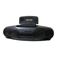
RX-DT30
n
Terminal Function of
ICs
l
IC702
(MN66271 RA)
Servo Processor
/
Digital Signal Processor
/
I
I
I
I
Pin
Mark
I/O
Function
No.
1
BCLK
0 Serial bit clock terminal (Not used, open)
2
LRCK
0
L/R
discriminating signal (Not used, open)
3
SRDATA
0 Serial data (Not used, open)
4
DVDD1
I
Power
supply
(digital circuit) terminal
5
DVSS1
(
-
1
GND (digital circuit) terminal
I
I
I
6
TX
0 Digital audio interface signal
I
I
I
7 MCLK
I
Microprocessor command clock signal
I
I
I
8 MDATA
I Microprocessorcommanddatasignal
9 MLD
I
Microprocessor command loadsignal
10
11
12
13
14
15
16
17
SENSE 0
Sense signal output
(OFT,FESL,MAGEND,NAJEND,FQSAD,SFG)
/FLOCK
0 Optical servo condition(focus)(‘L’
:
lead-in)
/TLOCK
0 Optical
servo condition(tracking)(“L”
:
lead-in)
BLKCK
0 Sub-code block clock (f=75Hz)
External clock signal input for sub-code Cl
SQCK
1
register
SUBQ
0 Sub-code
Q
code output
DMUTE
I
Muting input
(“H”
:
mute)
Status signal output
STAT
0 (CRC,CUE,CLVS,lTSTVP,FCLV,SQCK)
18
-
19
/RST
SMCK
I Reset input
1/2_divided
clock signal of crystal oscillating at
0
MSEL=‘H”
(fSMCK=8.4672MHz)
1/4-divided
clock signal of crystal
oscillating
at
MSEL=“L’(fSMCK=4.2336MHz)
20
PMCK
0
1/1
92-divided
clock signal of crystal
oscillating(fPMCK=88.2kHz)
(Not used, open)
21
TRV
0 Traverse servo control output
22
TVD
0 Traverse drive signal output
23
PC
0 Spindle motor ON signal output (‘L” : ON)
24
ECM
0
Spindle
motordrive
signal output
(forced mode output)
-- -^_
Spindle motordrive signal output
25
ECS
26
KICK
27
TRD
0
(servo error signal output)
0 Kick pulse output
0 Tracking drive output
I
I
I
I
28
FOD
0 Focus drive output
29
VREF
I
D/A (drive) output
(TVD,ECS,TRD,FOD,
FBAL,TBAL)
Reference voltage
input.
Digital Filter
/
D/A Converter
I
,
1
1
I
Pin
Mark
I/O
No.
Function
30 FBAL
o
Focus balance adjustment output
(Not
used,open)
31
TBAL
0 Tracking balanceadjustmentoutput
32
FE
I
Focus error
signal
input (analog input)
33
TE
I
Tracking error signal input (analog input)
34 RFENV
I
RF envelope signal input
I
I I
I
I
35 VDET
I
Vibration detection signal input (“H”
:
detection)
36 OFT
I
Off-track signal input (“H”
:
off track)
I
,
I
1
(fPCK=4.321
MHz during normal playback)’
54
PDO
I
0
IPhasecompansonsignalof
EFM and PCK
signals (Not used, open)
55 SUBC
0 Sub-code serial data output (Not used, open)
56
SBCK
I
Clock input for sub-code serial data
(Not used. open)
57
vss
-
GND
58
Xl
I
Crystal oscillating circuit input
(f=16.9344MHz)
59
60
/
X2
0 Crystal oscillating circuit output
(f=16.9344MHz)
VDD
I
Power supply input (foroscillating circuit)
-26-
 Loading...