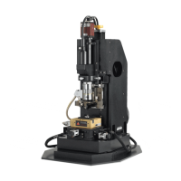
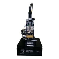
Preface
The Scanning Probe Microscope (SPM) is not only at the top of the list of equipment
pioneering the nano scale world, it is also the most fundamental technology.
Succeeding the first generation optical microscope, and the second generation
electron microscope, the SPM has every right to be known as a “third generation”
microscope since it enables us to look into the nano scale world. At the same time it
has many advantages over manual microscopes which passively observe samples.
The SPM is like a miniature robot, fabricating specific structures by manipulating
atoms on the sample surface and using a probe tip to take measurements of those
structures.
The SPM originated with the invention of the Scanning Tunneling microscope (STM).
The STM uses a tunneling current between a probe tip and a sample in a vacuum
state to measure surface topography. As a result, it is limited in that it can only
measure a sample which is a conductor or a semiconductor. Once the Atomic Force
Microscope (AFM) was developed, however, a whole new range of measurement
capabilities became possible. Now it is not only possible to measure non-conductors
in air, but also to measure the physical, chemical, mechanical, electrical, and
magnetic properties of a sample’s surface, and even measure live cells in solution.
The SPM is indeed the key to entering the world of nano technology that has yet to
flourish, and it is an essential equipment for various researches in the basic sciences
– physics, chemistry, and biology - and in applied industry - mechanical and electrical
engineering.
The importance of the SPM stands only to grow greater and greater in the future.


 To Next Page