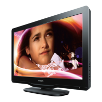
Do you have a question about the Philips 32PFL3508G/78 and is the answer not in the manual?
Details on product specifications, including connectivity options and available features.
Information on how to access product support and download user manuals.
Overview of all input/output ports and their functions for various TV series.
Essential safety regulations and procedures to follow during repair work.
Important warnings regarding ESD, high voltage, and component handling during repair.
General notes on measurements, waveforms, and schematic conventions.
Guidelines for measuring voltages and waveforms, including test signal details.
Conventions used in schematics for component values and notations.
Guidance on consulting the Philips Spare Parts Web Portal for component information.
Information on handling BGA devices and temperature profiles for repair.
Rules and best practices for working with lead-free soldering technology.
Explanation of how serial number digits indicate different Bill of Materials (BOM).
Alphabetical list of abbreviations used in the manual with their meanings.
Diagrams illustrating cable routing for various TV series to ensure proper assembly.
Guidelines for safely placing the TV set on a flat surface for servicing and measurements.
Step-by-step instructions for removing the rear cover and accessing internal components.
Procedure for safely disconnecting cables and removing the rear cover.
Instructions for disconnecting and removing the Small Signal Board (SSB).
Notes on removing Ambilight units, including adhesive residue.
General instructions for reassembling the TV set after repair, emphasizing cable management.
Identification of test points in schematics and layouts for diagnostic measurements.
Overview of different service modes (SDM, SAM, CSM, ComPair) for repair and diagnostics.
General information applicable to all service modes and navigation.
Details on activating and using SDM for measurements under uniform conditions.
Instructions for activating and using SAM for option settings and alignments.
Information on entering CSM for diagnosis, which displays operational settings.
Details on service tools like ComPair for diagnostics and software upgrades.
Introduction to ComPair, its functionalities, and connection requirements.
Explanation of error codes and how they indicate TV set failures.
Purpose of error codes and how they are stored in the error buffer.
Methods for reading the error buffer via OSD, blinking LED, or ComPair.
Table listing layer 1 error codes and their corresponding defective boards.
Procedures for clearing the error buffer using SAM or remote control commands.
Procedure for displaying errors using the front LED blinking sequence.
Explanation of how the blinking LED procedure indicates errors when OSD is not functional.
General tips and specific troubleshooting advice for common issues.
Using the NVM Editor in SAM mode to change NVM contents.
Procedure to initialize NVM with default values when replacing the NVM IC.
Troubleshooting steps for cases where the TV has no picture.
Checking HDMI EDID data for unstable picture issues.
Troubleshooting steps for no picture issues specifically via HDMI input.
Steps to enable Easylink for HDMI CEC functionality.
Troubleshooting for the TV failing to start up from standby mode.
Technical note regarding the tweeter signal measurement.
Technical note on expected low output at the tweeter connector.
Troubleshooting steps for no sound output from the class D amplifier.
Troubleshooting steps for no picture in analog RF mode.
Troubleshooting steps for no picture in digital RF mode.
Common issues and solutions for USB connectivity and device detection.
Troubleshooting steps for Ethernet link establishment and network connection.
Troubleshooting steps for HDMI connectivity, HDCP, and CEC issues.
Procedure for checking and adapting Ambilight parameters in NVM via SAM.
Instructions for pairing or unpairing the remote control unit with the TV.
Step-by-step guide for pairing the remote control unit to the TV.
Steps to unpair the remote control unit from the TV.
Information on upgrading the TV's main software via the USB port.
Overview of the possibility to upgrade main software via USB.
Procedure for performing an automatic software upgrade using 'autorun.upg'.
Instructions for copying NVM data between the TV and a USB stick.
Instructions for copying EDID data between the TV and a USB stick.
Instructions for copying the channel list data between the TV and a USB stick.
Conditions required for performing electrical alignments, including power supply and warm-up.
Statement that no hardware alignments are foreseen for this chassis.
Procedure for aligning RGB settings using the Service Alignment Mode (SAM).
Information on tuner AGC adjustment, noting it's automatic.
Detailed steps for RGB alignment, including picture settings and white tone adjustment.
Explanation of how option codes configure microprocessor communication with I2C ICs.
Introduction to option codes and their role in identifying specific ICs or functions.
Procedure to set option codes via SAM, referencing the sticker inside the cabinet.
Table listing display codes for various CTN and Panel Types.
Rule for defining cable position numbers based on connector and sourcing board.
Overview of the L12M3.1L LA chassis, Mediatek chipset, and key components.
Internal block diagram and pin configuration for the SUT-RA214 tuner IC.
Internal block diagram and pin configuration for the CXD2828 tuner/demodulator IC.
Internal block diagram of the MT5396 SoC, showing its key functions and interfaces.
Wiring diagram showing connections for 32-inch TVs in the 3500 series.
Wiring diagram illustrating connections for 32-inch TVs in the 4500 series.
Wiring diagram showing connections for 39-inch TVs in the 3500 series.
Wiring diagram illustrating connections for 39-inch TVs in the 4500 series.
Wiring diagram showing connections for 42-inch TVs in the 3500 series.
Wiring diagram illustrating connections for 42-inch TVs in the 4500 series.
Wiring diagram for 42/46-inch TVs in the 5000/5500 series.
Wiring diagram illustrating connections for 46-inch TVs in the 4500 series.
Wiring diagram showing connections for 47-inch TVs in the 7000 series.
Wiring diagram illustrating connections for 47-inch TVs in the 8000 series.
Wiring diagram showing connections for 55-inch TVs in the 7000 series.
Wiring diagram illustrating connections for 55-inch TVs in the 8000 series.
High-level block diagram of the MT5396 SoC and its main interfaces.
Block diagram for the MT5396 SoC, detailing interfaces and peripherals.
Circuit diagrams and PWB layouts for the 715G5778 Power Supply Unit.
Schematic diagram of the power circuit (A01) for the 715G5778 PSU.
Schematic diagram of the converter circuit (A02) within the 715G5778 PSU.
Top-side PWB layout for the 715G5778 Power Supply Unit.
Bottom-side PWB layout for the 715G5778 Power Supply Unit.
Circuit diagrams and PWB layouts for the 715G5792 Power Supply Unit.
Schematic diagram of the AC input section (A01) of the 715G5792 PSU.
Schematic diagram of the Power Factor Correction (PFC) circuit (A02).
Schematic diagram of the main power stage (A03).
Schematic diagram for the D2D LED Driver circuit (A04).
Schematic diagram for the LED Current Balance circuit (A05).
Top-side PWB layout for the 715G5792 PSU.
Bottom-side PWB layout for the 715G5792 PSU.
Circuit diagrams and PWB layouts for the 715G5793 Power Supply Unit.
Schematic diagram of the power section (A01) for the 715G5793 PSU.
Schematic diagram of the LED Driver circuit (A02).
Top-side PWB layout for the 715G5793 PSU.
Bottom-side PWB layout for the 715G5793 PSU.
Circuit diagrams and PWB layouts for the ALC 715G6001 Option Board.
Schematic diagram of the ALC Option Board.
Layout diagrams for the top and bottom sides of the Option Board.
Circuit diagrams and PWB layouts for the 313912365441 SSB board.
Schematic diagram of the DC-DC converters on the SSB board.
Schematic diagram of the tuner and demodulator section.
Schematic diagram of the Class-D audio amplifier and muting circuit.
Schematic diagram showing power distribution for the MTK5396 SoC.
Schematic diagram of the DDR3 memory interface connections.
Schematic for Flash memory, control signals, EJTAG, and Ambilight.
Schematic diagram for the LVDS display interface connections.
Schematic diagram for the HDMI input/output ports.
Schematic diagram for the USB ports and related circuitry.
Schematic diagram for the headphone output circuitry.
Schematic diagram for Component and Composite video inputs.
Schematic diagram for the VGA input and its associated components.
Schematic diagram for the Ethernet port and related circuitry.
Top-side PWB layout for the 313912365441 SSB board.
Bottom-side PWB layout for the 313912365441 SSB board.
Circuit diagrams and PWB layouts for the 313912365451 SSB board.
Schematic diagram of DC-DC converters on the SSB board.
Schematic diagram of the tuner and demodulator section.
Schematic diagram of the Class-D audio amplifier and muting circuit.
Schematic diagram showing power distribution for the MTK5396 SoC.
Schematic diagram of the DDR3 memory interface connections.
Schematic for Flash memory, control signals, EJTAG, and Ambilight.
Schematic diagram for the LVDS display interface connections.
Schematic diagram for the HDMI input/output ports.
Schematic diagram for the USB ports and related circuitry.
Schematic diagram for the headphone output circuitry.
Schematic diagram for Component and Composite video inputs.
Schematic diagram for the VGA input and its associated components.
Schematic diagram for the Ethernet port and related circuitry.
Top-side PWB layout for the 313912365451 SSB board.
Circuit diagrams and PWB layouts for the Keyboard Control Module.
Schematic diagram of the Keyboard Control Module.
Layout of the Keyboard Control Panel (top and bottom sides).
Circuit diagrams and PWB layouts for the E 715G5771 board.
Schematic diagram of the keyboard control panel.
Layout of the keyboard control panel (top and bottom sides).
Circuit diagrams and PWB layouts for the J 715G5783 IR/LED panel.
Schematic diagram of the IR/LED panel.
Layout of the IR/LED panel (top and bottom sides).
Circuit diagrams and PWB layouts for the J 715G5820 IR/LED panel.
Schematic diagram of the IR/LED panel.
Layout of the IR/LED panel (top and bottom sides).
Circuit diagrams and PWB layouts for the Sensor Module.
Schematic diagram of the RF4CE Sensor Module.
Circuit diagrams and PWB layouts for the 7 LED Master LiteOn Ambilight.
Schematic diagram for the AL1 7 LED Master LiteOn Ambilight module.
Circuit diagrams and PWB layouts for the 9 LED LiteOn Ambilight.
Schematic diagram for the AL1 9 LED LiteOn Ambilight module.
Circuit diagrams and PWB layouts for the 8 LED Everlight Ambilight.
Schematic diagram for the AL1 8 LED Everlight Ambilight module.
Circuit diagrams and PWB layouts for the 7 LED Everlight Ambilight.
Schematic diagram for the AL1 7 LED Everlight Ambilight module.
Circuit diagrams and PWB layouts for the 8 LED Everlight Ambilight.
Schematic diagram for the AL1 8 LED Everlight Ambilight module.
Circuit diagrams and PWB layouts for the 8 LED Everlight Ambilight.
Schematic diagram for the AL2 8 LED Everlight Ambilight module.
Exploded view and parts list for the 3500 series 32-inch TV.
Exploded view and parts list for the 4500 series 32-inch TV.
Exploded view and parts list for the 3500 series 39-inch TV.
Exploded view and parts list for the 4500 series 39-inch TV.
Exploded view and parts list for the 3500 series 42-inch TV.
Exploded view and parts list for the 4500 series 42-inch TV.
Exploded view and parts list for 5000/5500 series 42/46-inch TVs.
Exploded view and parts list for the 4500 series 46-inch TV.
Exploded view and parts list for 7000 series 47/55-inch TVs.
Exploded view and parts list for the 8000 series 47-inch TV.
Exploded view and parts list for the 8000 series 55-inch TV.
