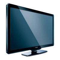
Do you have a question about the Philips 42ta648bx/37 and is the answer not in the manual?
Details display, resolution, contrast, viewing angles, and sound specifications.
Describes side and rear I/O ports, including HDMI, USB, AV, and antenna connections.
Illustrates the internal PWB/CBA locations for different screen sizes.
Outlines essential safety regulations for performing repairs on the set.
Highlights critical warnings regarding ESD, high voltage, and component handling during repair.
Provides general notes on measurements, schematic symbols, BGA ICs, and soldering.
Explains how the third digit of the serial number identifies the Bill Of Materials (BOM) used.
Discusses whether to exchange or repair boards, emphasizing OEM return policies.
Offers essential precautions for service, including electrical shock avoidance and high voltage insulation testing.
Provides website links for downloading service information and manuals.
Provides detailed illustrations and instructions for routing internal cables correctly during assembly.
Describes recommended set positions and foam bar usage for easier and safer servicing.
Details the procedure for removing the back cover and accessing internal components, with warnings.
Outlines the steps for reassembling the set, emphasizing cable placement and EMC foam.
Explains how test points are indicated in schematics and layouts for diagnosis.
Describes various service modes (SDM, SAM, CSM, ComPair) and their functions for repair.
Introduces ComPair as a Windows-based tool for diagnostics and software upgrades.
Explains the error buffer and how error codes indicate TV failures.
Details how to interpret front LED blinking sequences for error identification.
Offers general advice on software protections, hardware protections, and NVM editor usage.
Guides on upgrading TV software using a USB port and the "autorun.upg" file.
Provides a detailed wiring diagram for the 32-inch ME8/MG8 models.
Presents a detailed wiring diagram for the 42" and 47" ME8/MG8 models.
Offers a detailed wiring diagram for the 52-inch ME8/MG8 models.
Illustrates the video signal flow and processing within the chassis.
Depicts the audio signal path and processing stages.
Shows the flow of control and clock signals across the system.
Locates test points on the Small Signal Board (SSB) bottom side for troubleshooting.
Details the I2C communication paths between ICs on the SSB.
Provides an overview of the power supply lines distributed throughout the SSB.
Shows the schematic and PWB layout for the DC/DC converter circuit.
Presents the circuit diagram and PWB layout for the tuner and demodulator.
Details the circuit and PWB layout for the Class-D audio amplifier and muting circuit.
Provides the circuit diagram and PWB layout for the MT5382 power and tuner sections.
Shows the circuit and PWB layout for the MT5382 DDR2 SDRAM connections.
Presents the circuit and PWB layout for the MT5382 flash memory and NVM.
Details the circuit and PWB layout for the MT5382 LVDS interface.
Shows the circuit and PWB layout for the MT5382 HDMI inputs and multiplexer.
Presents the circuit and PWB layout for the MT5382 analog input/output connections.
Details the circuit and PWB layout for the MJC MT8280 power supply interface.
Shows the circuit and PWB layout for the MJC MT8280 DDR2 memory connections.
Presents the circuit and PWB layout for the MJC MT8280 LVDS interface.
Provides the circuit and PWB layout for the Ambilight FPGA module.
Shows the circuit and PWB layout for the reserved ITV Channel Decoder.
Details the circuit and PWB layout for the reserved ITV Pro:Idiom module.
Explains the Service Reference Protocol (SRP) list used for signal tracing.
Lists signal references and their schematic locations as per SRP.
Provides an overview of the SSB layout, divided into sections.
Shows the component placement on the top side of SSB Part 1.
Details component placement on the top side of SSB Part 2.
Illustrates component placement on the top side of SSB Part 3.
Shows component placement on the top side of SSB Part 4.
Details component placement on the bottom side of SSB Part 1.
Illustrates component placement on the bottom side of SSB Part 2.
Shows component placement on the bottom side of SSB Part 3.
Details component placement on the bottom side of SSB Part 4.
Provides circuit diagrams and PWB layouts for the keyboard control panel.
Shows the circuit diagram and PWB layout for the IR and LED panel.
Illustrates the component layout for the IR & LED panel (top side).
Outlines the necessary conditions and settings for performing electrical adjustments.
States that no hardware alignments are foreseen for this chassis.
Details how to perform software alignments, including white tone and RGB adjustments.
Explains the procedure for RGB alignment, including white tone and black level offset.
Guides on setting option codes to configure the TV for specific hardware and features.
Introduces the LC8.1U chassis, its development name, and key components.
Describes the PSU unit, its types, and voltage outputs to the chassis.
Details the on-board DC-DC converters and the voltages they supply to the SSB.
Explains the tuner and signal processing for analog and digital reception.
Describes the video signal processing path within the MT5382 processor.
Details the audio signal processing performed by the MT5382 processor.
Explains the HDMI implementation, receivers, CEC support, and connectors.
Describes the location and implementation of AmbiLight units.
Overviews the control signal flow for the LC08SP platform, including GPIO functions.
Provides a comprehensive list of abbreviations used throughout the document.
Shows internal block diagrams and pin configurations for key ICs.
