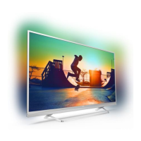
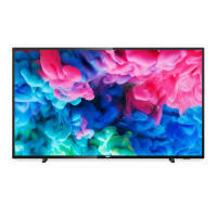
Do you have a question about the Philips 43PUS6432/12 and is the answer not in the manual?
Details technical specifications for TV models: energy efficiency, screen size, power consumption, and resolution.
Lists connectors on the TV's side panel: HDMI, USB, and common interface slot.
Lists connectors on the TV's rear panel: Audio In, SCART, and YPbPr.
Lists connectors on the TV's bottom panel: HDMI, USB, and audio out.
Illustrates cable routing for different TV series (43" 6432, 43" 7202).
Instructions for removing the rear cover, including screw locations and connector disconnections.
Steps to release clamps and unplug connectors for ambilight panels and keyboard FFC.
Instructions for releasing connectors and removing fixation screws for the keyboard control panel.
Procedures for releasing LVDS and other connectors, and removing SSB fixation screws.
Steps to unplug connectors, remove fixation screws, and take out the PSU.
Instructions for removing fixation screws, releasing covers, and unplugging connectors for the IR/LED board.
Steps to release tapes, unplug speaker connectors, and remove speakers.
Instructions for unplugging connectors and removing fixation screws for the WIFI module.
Detailed steps for removing the LCD Panel, including fixations screws and other parts.
Instructions for removing fixation screws and sliding out the IR/LED Board.
Steps to remove screws securing the black plastic casing and Allen screws for the stand bracket.
Instructions for removing fixation screws and unplugging the connector from the SSB to lift the rear cover.
Steps to release clamps and unplug connectors for ambilight panels and keyboard FFC.
Instructions for releasing connectors and removing fixation screws for the keyboard control panel.
Procedures for releasing LVDS and other connectors, and removing SSB fixation screws.
Steps to unplug connectors, remove fixation screws, and take out the PSU.
Instructions for removing fixation screws, releasing covers, and unplugging the connector for the LED Logo board.
Explains different service modes (SAM, Factory, CSM) and their purposes for engineers and consumers.
Details purpose, specifications, and activation methods for Service Alignment Mode.
Details purpose and specifications of Factory Mode for extended alignments and settings.
Explains purpose and specifications of CSM for customer diagnosis and error code reporting.
Step-by-step instructions for preparing and performing a firmware upgrade via USB.
Explains purpose of error codes, the error buffer, and how failures are identified and displayed.
Explains how to set the panel code using a remote sequence and lists panel types and their codes.
Introduces the QM17.3E LA chassis, MT5593U+ platform, and supported stylings.
Lists key components of the chassis, such as scalers, demodulators, and flash memory.
A high-level block diagram showing interconnections of major components like CPU, memory, and interfaces.
Describes power supplies, ordering procedures, and platform delta features like LED backlight architecture.
Lists on-board DC/DC converters and the voltages they deliver depending on set execution.
Details key components for the front-end analogue tuner and a block diagram for DVB-C.
Lists key components for the DVT front-end and provides a block diagram for DTV reception.
Lists HDMI connectors and their supported features like HDCP, MHL, and ARC.
Provides a block diagram of the MT5593UGIJ IC, showing its functional blocks and interfaces.
Block diagram and pin assignments for the SI2169-C50 demodulator IC.
Block diagram and pin assignments for the TAS5760LDDCAR audio amplifier IC.
Circuit diagram for the AC input section of the 715G7350 PSU used in 43" 6432 series models.
Circuit diagram for the AC input section of the 715G6973 PSU used in 49"/55" 6432 and 49" 7272 series.
Circuit diagram for the AC input section of the 715G7857 PSU used in 43" 7202 series models.
Circuit diagram for the AC input section of the 715G7312 PSU used in 55" 7272 series models.
Circuit diagram for the SOC-EMMC section, detailing its power, interface, and memory components.
Pin assignments and decoupling/reference voltage circuits for MT5593 DDR3 memory modules.
Pin assignments and decoupling/reference voltage circuits for MT5593 DDR3 memory modules.
Pin assignments and decoupling/reference voltage circuits for MT5593 DDR3 memory modules.
Details key components for the front-end tuner and block diagrams for DVB-C and DTV reception.
Pin assignments and input/output diagrams for the NT72333 Vx1 interface.
Diagrams and explanations for NT324 GPIO functionalities, including programming and strapping.
Diagrams for NT324 V-BY-1 output and +12V-DISP connections.
Circuit diagrams for NT324 power supply, showing various voltage rails and filtering.
VREF voltage divider circuits for NT324 DDR memory interfaces.
Pin assignment diagram for NT324, focusing on GND pins and their connections.
Circuit diagrams for Novatek DCDC converters, detailing power supply for various voltage rails.
Power supply circuits for VCCK and 3V3 IO rails, showing capacitor filtering and SoC connections.
Circuit diagrams for system power DC-DC converters, including DRAM power, TUNER VCC, and DV12.
Circuit diagrams for system power DC-DC converters, covering Wi-Fi, Ambilight, and LNB power supply.
Circuit diagrams for the first-class D-AMP audio system, including mute circuits and SPDIF output.
Circuit diagrams for the second-class D-AMP audio system, detailing mute circuits and audio module SPDIF output.
Diagrams for SOC GPIO pins, PCMCIA slot, CI slot power control, and bus power control.
Diagrams showing HDMI connections to RX ports, including ESD and surge protection circuits.
Diagrams illustrating HDMI signal routing from SOC to connectors and the Audio Return Channel (ARC) circuit.
Circuit diagrams for SCART, YPbPr, and CVBS inputs, including audio and video signal routing.
Diagrams showing connections for AL+KEY, Wordmark Driver, Debug IR receiver, and Sensor Board.
Diagrams for Ethernet PHY, Wi-Fi control, USB ports, and USB camera connections.
Diagrams for HTV connections, including speaker output, IR IN/OUT, RS232, and 12V protection.
Diagrams illustrating IR/LED panel components, 3D de-interference, and light sensor.
Diagrams showing standby LED, IR receiver, and light sensor components for the 715G8009 panel.
Diagrams showing standby LED, IR receiver, and light sensor components for the 715G8010 panel.
Defines joystick key functions and provides a circuit diagram and diversity table for the keyboard.
Styling sheet showing exploded view of 43" 6432 TV and parts list with position numbers.
Styling sheet showing exploded view of 43" 7202 TV and parts list with position numbers.
Styling sheet showing exploded view of 49" 6432 TV and parts list with position numbers.
Styling sheet showing exploded view of 49" 7272 TV and parts list with position numbers.
Styling sheet showing exploded view of 55" 6432 TV and parts list with position numbers.
Styling sheet showing exploded view of 55" 7272 TV and parts list with position numbers.


