Do you have a question about the Pira P275 and is the answer not in the manual?
User guide for FM Scope software.
Software for RDS decoding on Windows.
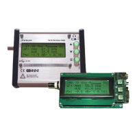
Key features and design aspects of the P275 FM Broadcast Analyzer.
List of measurements, indications, and audio outputs provided by the device.
Manufacturer's liability for damages and product use.
Copyright notice and document revision information.
Declaration of compliance with European Directives and product standards.
Details of EMC testing performed on the device.
General parameters like supply voltage, current, dimensions, and CPU.
Technical details for the RF input, including impedance, frequency range, and sensitivity.
Specifications for frequency deviation, modulation power, and RDS deviation.
Technical parameters for the MPX input, such as impedance and bandwidth.
Current limits and specifications for alarm output pins.
Specifications for audio output channels, impedance, and level.
Details on RDS filter, demodulator, and supported RDS groups.
RDS deviation parameters and antenna input sensitivity for RDS.
Description of the BNC input and USB Micro connectors.
Details on the battery compartment and RS-232 serial port connector.
Information on the power switch and alarm output pin header.
Details on the 3.5mm audio output jack.
Using the USB Micro connector for device power.
Using the battery connector for device power with NiMH cells.
Power supply inputs via internal connectors (J2, J3, J17).
Detailed pin assignments for various connectors on the mainboard.
Pinout for the LCD connector (CONLCD1).
Pinout and function of the J3 optional control interface.
Pinout and control functions for the J4 optional CPU interface.
Note regarding the absence of adjusting elements on the board.
Important note on using multiple serial communication ports simultaneously.
Table defining conditions and interpretations for alarm outputs.
Graphical example illustrating alarm response timing and hysteresis.
Application example showing logical sum (OR function) of alarm outputs.
Steps and requirements for powering up the device.
Explanation of control buttons and how to navigate the menu system.
Detailed list of available menu items and their functions.
How to switch between RF and MPX input signals and display changes.
Procedure for saving measurements to internal EEPROM memory.
Procedure for loading saved measurements and using them as presets.
How to adjust the audio volume for headphones output.
Warning and procedures for low battery conditions.
Parameters and influences that determine the signal quality indication.
Scale illustrating signal level versus reception quality and measurement ability.
Table mapping signal quality symbols to their meaning.
Tables showing max measuring distance based on ERP and antenna type.
Factors influencing antenna choice and suitability of different antenna types.
Advice on antenna placement and avoiding interference sources.
Guidance on using the transmitter's RF test output for measurements.
How PC signals and data cables can interfere with measurements.
Method to mitigate interference by coiling data cables.
Explanation of MAX, AVE, MIN values and hold functions for peak deviation.
The maximum allowed peak frequency deviation value.
Role of the 19 kHz pilot tone in stereo FM transmission.
The typical range for carrier deviation caused by the pilot tone.
How phase difference is measured and its acceptable tolerance.
What to check if RDS and pilot are not in stable phase relation.
Formula and definition of modulation power averaged over 60 seconds.
Typical modulation power limits and how the 'Pm' symbol indicates accuracy.
Step-by-step process for generating the frequency deviation histogram.
How to interpret the histogram and notes on its display.
Explanation of 'Signal' and 'Noise/AM' values.
Causes and impact of AM modulation on the signal.
How to display and interpret the stereo balance meter.
Procedure to determine carrier frequency offset using the device.
An example illustrating how to read and interpret carrier offset values.
How basic RDS information is shown on the device.
Information on block error rate and received RDS groups.
How to access detailed RDS information and group content viewer.
How the group order buffer displays and locks RDS group sequences.
How group content is displayed after reception.
Specific display for group type 3a (ODA AID).
Summary of services and functions available on RDS sub-pages.
Table of RDS services and whether they are decoded by the device.
List of ODA (Open Data Applications) with their AIDs and names.
Errors related to the first and second PI digits and their solutions.
Errors related to AF list and single transmitter PI digits.
How to connect the FM analyzer to a PC using RS-232 or USB.
Recommended communication parameters for PC connection.
Explanation of the autobaud feature for communication speed.
List of commands for tuning, saving, enabling measurements, and reset.
Commands for setting DIP switches, alarm registers, and memory.
Commands to retrieve basic data, frequencies, deviation, and RDS info.
Commands for retrieving memory content, version, and carrier offset.
Configuration options controlled by DIP switches.
Details on alarm registers for silence, overmodulation, pilot, and RDS errors.
Settings for alarm time duration, hysteresis, and signal lost.
Using the software tool to configure alarm outputs and settings.
How to use special values to force alarm outputs to low or high state.
Using alarm outputs to control external circuits.
Using alarm pins to follow the RDS TA (Traffic Announcement) state.
Definition of the data format returned by the device.
Mapping of keys to commands that retrieve specific data.
Mapping of keys to commands that control device functions.
Steps for updating the device firmware.
Using an external 10 MHz reference for accurate frequency offset measurement.
Detailed memory map of the device, including addresses, content, and units.
Summary of RDS data and list of RDS services.
Mechanical dimensions and layout of the mainboard.
Schematic example for connecting the J3 control interface.
| Brand | Pira |
|---|---|
| Model | P275 |
| Category | Measuring Instruments |
| Language | English |