5-4 Maintenance
5.3.1 PLL Frequency Adjustment5.3.1 PLL Frequency Adjustment
5.3.1 PLL Frequency Adjustment5.3.1 PLL Frequency Adjustment
5.3.1 PLL Frequency Adjustment
(Transmitter, All Channel Receiver)(Transmitter, All Channel Receiver)
(Transmitter, All Channel Receiver)(Transmitter, All Channel Receiver)
(Transmitter, All Channel Receiver)
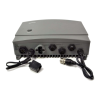
1) Connect the power supply (13.2V, 10A) to the DC Power Line.
2) Connect the RF Power Meter and a Frequency Counter through the
coupler.
3) Turn the radio "ON" and select Channel 16 (156.800 MHz).
4) Press PTT on the Handset and read the indication on the Frequency
Counter.
5) Adjust trimmer capacitor (TC1) on the RF PCB (see Fig 5-2) for the
desired frequency (156.800 MHz) +/- 100 MHz.
5.3.2 Local Oscillator Adjustment (Channel5.3.2 Local Oscillator Adjustment (Channel
5.3.2 Local Oscillator Adjustment (Channel5.3.2 Local Oscillator Adjustment (Channel
5.3.2 Local Oscillator Adjustment (Channel
70 Receiver)70 Receiver)
70 Receiver)70 Receiver)
70 Receiver)
1) Connect a Frequency Counter to TP1 on the RF PCB and GND.
2) Set the radio on Channel 16 and adjust trimmer capacitor (TC2) on the
RF PCB for the desired frequency (139.625 MHz) +/- 100Hz.
5.3.3 Modulation Adjustment (Transmitter)5.3.3 Modulation Adjustment (Transmitter)
5.3.3 Modulation Adjustment (Transmitter)5.3.3 Modulation Adjustment (Transmitter)
5.3.3 Modulation Adjustment (Transmitter)
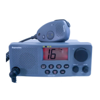
1) Connect an FM Linear Detector through the coupler.
2) Connect the Audio Oscillator to the IDC input (pin 15 of J2) as shown
in Fig 5-3.
3) Set the AF OSC output to 0 dBm (0.77 Vrms) at 1 kHz.
4) Press PTT and adjust VR3 on the RF PCB to the maximum modulation
of 4.5 kHz +/-100 Hz.5.3.4
5.3. Output Power Adjustment (Transmitter)5.3. Output Power Adjustment (Transmitter)
5.3. Output Power Adjustment (Transmitter)5.3. Output Power Adjustment (Transmitter)
5.3. Output Power Adjustment (Transmitter)
1) Connect the RF Power meter.
2) Set the radio on CH 16 (156.800 MHz) .
3) Transmit and adjust the RF power output by VR1 (Low) and VR2 (High)
on the RF PCB as follows.
SequenceSequence
SequenceSequence
Sequence
RF Power RF Power
RF Power RF Power
RF Power
Adjust Point Adjust Point
Adjust Point Adjust Point
Adjust Point
Target PowerTarget Power
Target PowerTarget Power
Target Power
1 Low VR1 0.9W +/- 0.05W (limit 1W)
2 High VR2 24W +/-0.5W (limit 25W)
 Loading...