October 2009
General Information DDR3 SDRAM
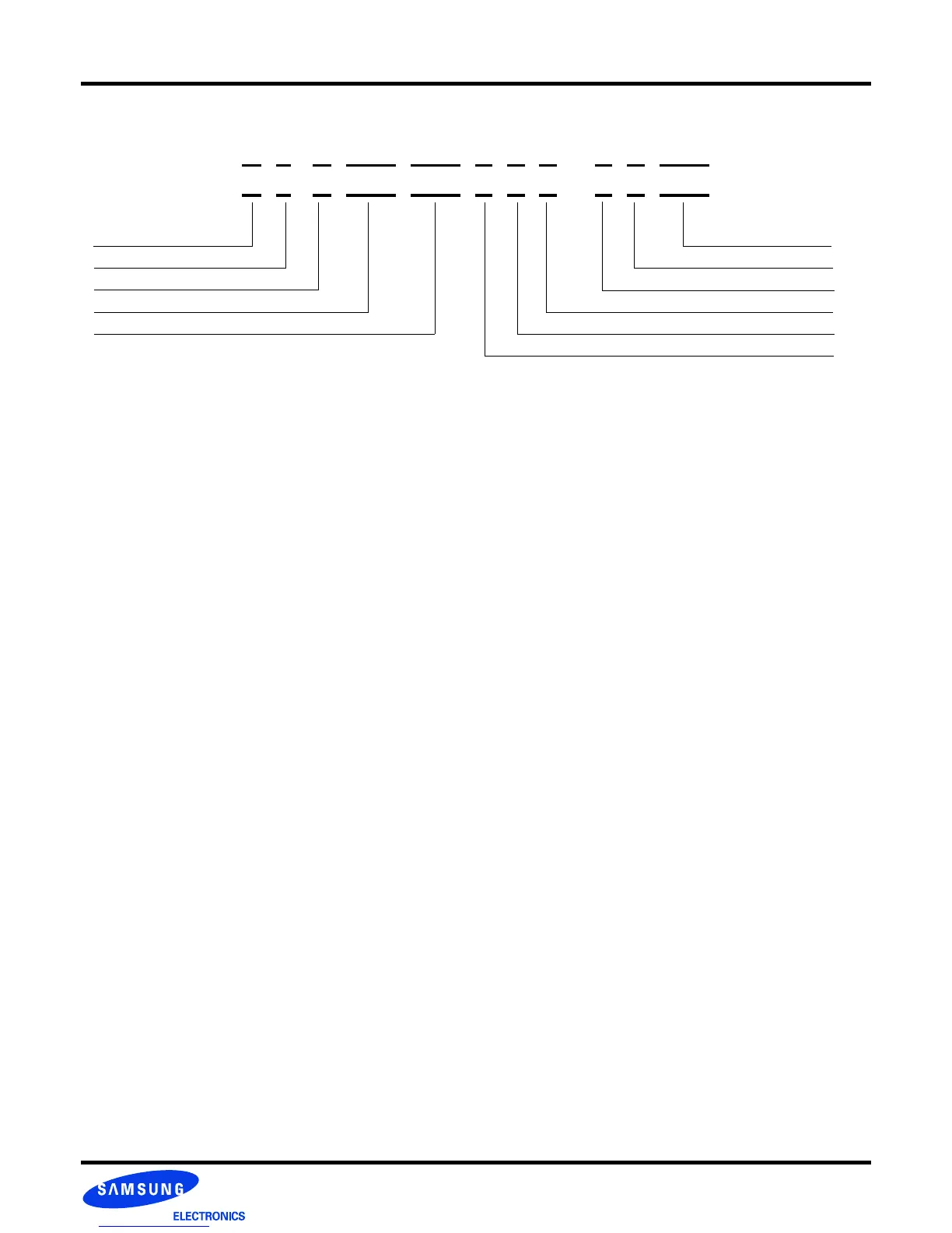
1. DDR3 SDRAM Component Ordering Information
51 : 512Mb
1G : 1Gb
2G : 2Gb
4G : 4Gb
04 : x 4
08 : x 8
16 : x16
3 : 4 Banks
4 : 8 Banks
5 : 16 Banks
3. DRAM Type
4. Density
5. Bit Organization
6. # of Internal Banks
M
A
B
C
D
E
F
G
H
Z
H
J
M
C
L
Y
9. Package Type
8. Revision
10. Temp & Power
1. SAMSUNG Memory : K
2. DRAM : 4
Revision
# of Internal Banks
Bit Organization
Density
DRAM Type
DRAM
SAMSUNG Memory
Interface (V
DD, VDDQ)
Package Type
Temp & Power
1 2 3 4 5 6 7 8 9 10 11
Speed
B : DDR3 SDRAM
: Commercial Temp.( 0°C ~ 85°C) & Normal Power
: Commercial Temp.( 0°C ~ 85°C) & Low Power
: Commercial Temp.( 0°C ~ 85°C) & Low VDD(1.35V)
: FBGA (Lead-free)
: FBGA (Halogen-free & Lead-free)
: FBGA (Lead-free, DDP)
: FBGA (Halogen-free & Lead-free, DDP)
: 1st Gen.
: 2nd Gen.
: 3rd Gen.
: 4th Gen.
: 5th Gen.
: 6th Gen.
: 7th Gen
: 8th Gen
: 9th Gen
11. Speed
K 4 B X X X X X X X - X X X X
: DDR3-800 (400MHz @ CL=6, tRCD=6, tRP=6)
: DDR3-1066 (533MHz @ CL=7, tRCD=7, tRP=7)
: DDR3-1333 (667MHz @ CL=9, tRCD=9, tRP=9)
: DDR3-1600 (800MHz @ CL=11, tRCD=11, tRP=11)
F7
F8
H9
K0
6 : SSTL (1.5V, 1.5V)
7. Interface ( V
DD, VDDQ)