S3C84I8/F84I8/C84I9/F84I9 ERRATA
2
ERRATA (VER 0.0)
Samsung 8-bit MCU S3C84I8/F84I8/C84I9/F84I9 User's Manual
Document Number: 21-S3-C84I8/F84I8/C84I9/F84I9-072006
Publication: July 2006
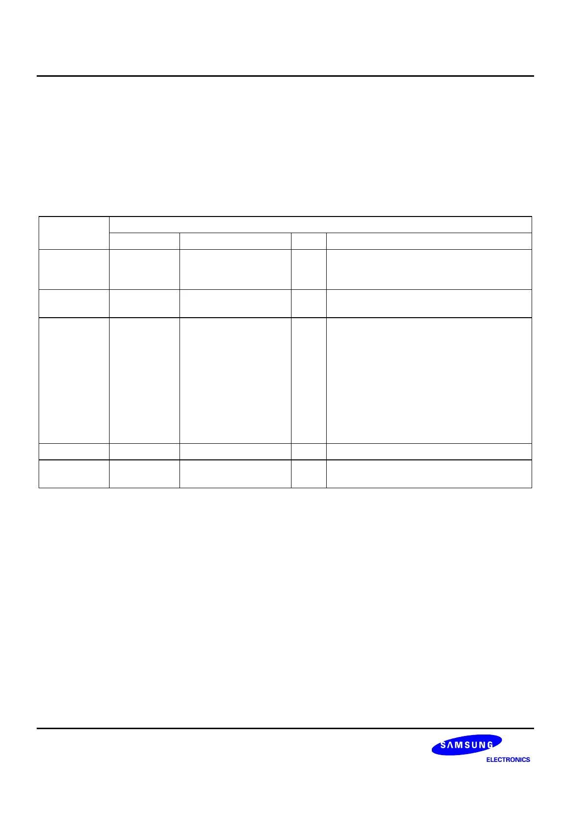
Table 20-1. Descriptions of Pins Used to Read/Write the Flash ROM
Main Chip During Programming
Pin Name Pin Name Pin No. I/O Function
P1.2 SDAT 3 (44-pin)
9 (42-pin)
I/O Serial data pin (output when reading, Input
when writing) Input and push-pull output port
can be assigned
P1.3 SCLK 4 (44-pin)
10 (42-pin)
I Serial clock pin (input only pin)
TEST
V
PP
4 I Power supply pin for flash ROM cell writing
(indicates that MTP enters into the writing
mode). When 12.5 V is applied, MTP is in
writing mode and when 5 V is applied,
MTP is in reading mode. (Option)
NOTE:
A 100pF capacitor must be connected between
Vpp and Vss when data in the flash ROM are
read or written by a tool (SPW2+, Gang
Writer)(S3F84I8 ONLY).
nRESET nRESET 7 I –
V
DD
/V
SS
V
DD
/V
SS
5 / 6 (44-pin)
11/12 (42-pin)
I Logic power supply pin.



 To Next Page