CD-E770
From
©
on
pagezyxwvutsrqponmlkjihgfedcbaZYXWVUTSRQPONMLKJIHGFEDCBA
10.
•
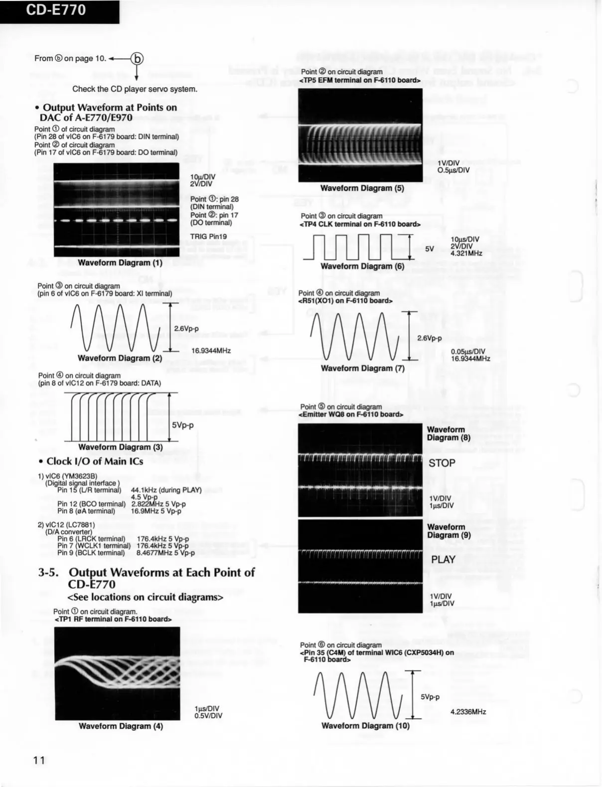
Point @ on circuit diagram
<TP5 EFM terminal on F-6110 board>
Check
the CD player
servo
system.
• Output Waveform
at
Points
on
DACof
A-E770/E970
Point
® of
circuit diagram
(Pin
28
of
vlC6 on F-6179 board: DIN terminal)
Point
® of
circuit diagram
(Pin
17
of
vlC6 on F-6179 board: DO terminal)
fMlllilHi:
^
lOu/DIV
2\//DIV
Point
®:
pin
28
(DIN
terminal)
Point®: pin
17
(DO
terminal)
TRIG
Pin19
1V/DIV
0.5MS/DIV
Waveform
Diagram (5)
Point
®
on circuit diagram
<TP4
CLK
terminal on F-6110 board>
Waveform
Diagram (1)
!
Point
®
on circuit diagram
(pin
6 of
vlC6 on F-6179 board: XI terminal)
5V
lOus/DIV
2V/DIV
4.321MHz
Waveform
Diagram (6)
Point
®
on circuit diagram
<R51(X01) on F-6110 board>
2.6Vp-p
Waveform
Diagram (2)
Point
®
on circuit diagram
(pin
8 of
vICI
2 on F-6179 board:
DATA)
16.9344MHz
2.6Vp-p
0.05MS/DIV
16.9344MHz
Waveform
Diagram (7)
Point
©
on circuit diagram
<Emitter WQ8 on F-6110 board>
5Vp-p
Waveform
Diagram (3)
Clock
I/O of
Main
ICs
1)vlC6
(YM3623B)
(Digital signal interface)
Pin
15
(17R
terminal)
44.1kHz
(during
PLAY)
4.5
Vp-p
- --2MH:
Pin
12
(BCO
terminal) 2.822MHz
5
Vp-p
Pin
8
(0A
terminal) 16.9MHz 5 Vp-p
2)vlC12{LC7881)
(D/A
converter)
Pin
6
(LRCK
terminal) 176.4kHz
5
Vp-p
,
Pin
7
(WCLK1
terminal) 176.4kHz
5
Vp-p
i
Pin
9
(BCLK
terminal) 8.4677MHz
5
Vp-p
3-5. Output Waveforms
at
Each
Point
of
CD-E770
<See locations on circuit diagrams>
Point
®
on circuit diagram.
<TP1 RF terminal on F-6110 board>
Waveform
Diagram
(8)
STOP
1V/DIV
l^s/DIV
Waveform
Diagram
(9)
PLAY
1V/DIV
lus/Dl
V
Point
©
on circuit diagram
<Pin
35 (C4M)
of
terminal WIC6 (CXP5034H) on
F-6110 board>
IMS/DIV
0.5V/DIV
5Vp-p
4.2336MHz
Waveform
Diagram (4)
Waveform
Diagram (10)
1
1
 Loading...