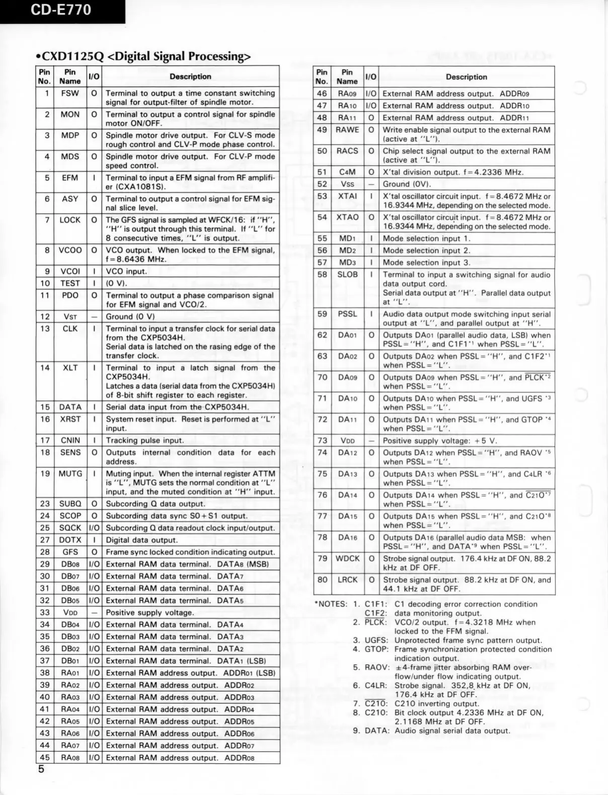
CD-E770
•CXD1125Q
<Digital
Signal Processing>
Pin
No.
Pin
Name
1/0
Description
1
FSW
0
Terminal
to
output
a
time constant switching
signal
for
output-filter
of
spindle motor.
2 MON 0 Terminal
to
output
a
control signal
for
spindle
motor ON/OFF.
3 MDP 0
Spindle motor drive output.
For
CLV-S mode
rough control
and
CLV-P mode phase control.
4 MDS 0
Spindle motor drive output.
For
CLV-P mode
speed control.
5
EFM
1
Terminal
to
input
a
EFM signal from RF amplifi-
er (CXA1081S).
6
ASY
0
Terminal
to
output
a
control signal
for
EFM
sig-
nal slice level.
7
LOCK
0 The GFS signal
is
sampled
at
WFCK/16:
if
"H",
"H"
is
output through this terminal.
If "L" for
8 consecutive times,
"L" is
output.
8 VCOO 0 VCO output. When locked
to the EFM
signal,
f
=
8.6436
MHz.
9
VCOl
1 VCO input.
10 TEST 1
(0
V).
11 PDO 0 Terminal
to
output
a
phase comparison signal
for
EFM
signal
and
VCO/2.
12
VST
—
Ground
(0 V)
13
CLK
1
Terminal
to
input
a
transfer clock
for
serial data
from
the
CXP5034H.
Serial data
is
latched
on the
rasing edge
of the
transfer clock.
14 XLT
1
Terminal
to
input
a
latch signal from
the
CXP5034H.
Latches
a
data (serial data from
the
CXP5034H)
of
8-bit
shift register
to
each register.
15 DATA 1
Serial data input from
the
CXP5034H.
16 XRST 1 System reset input. Reset
is
performed
at "L"
input.
17 CNIN
1
Tracking pulse input.
18 SENS 0
Outputs internal condition data
for
each
address.
19 MUTG 1
Muting input. When
the
internal register ATTM
iszyxwvutsrqponmlkjihgfedcbaZYXWVUTSRQPONMLKJIHGFEDCBA
"L",
MUTG sets
the
normal condition
at "L"
input,
and the
muted condition
at "H"
input.
23 SUBQ 0 Subcording
Q
data output.
24
SCOP 0 Subcording data sync S0-^S1 output.
25
SQCK
1/0
Subcording
O
data readout clock input/output.
27 DOTX
1 Digital data output.
28 GFS 0 Frame sync locked condition indicating output.
29 DBo8
1/0
External
RAM
data terminal. DATAs
(MSB)
30
DB07
1/0
External
RAM
data terminal. DATA?
31 DBo6
1/0
External RAM data terminal.
DATAe
32
DBo5
1/0
External RAM data terminal.
DATA5
33
VDD
-
Positive supply voltage.
34
DBo4
1/0
External RAM data terminal.
DATA4
35
DB03
1/0
External RAM data terminal.
DATA3
36
DB02
1/0
External RAM data terminal.
DATA2
37
DBoi
1/0
External RAM data terminal.
DATAi
(LSB)
38
RAoi
1/0
External RAM address output.
ADDRoi
(LSB)
39
RAo2
1/0
External RAM address output.
ADDR02
40
RA03
1/0
External RAM address output.
ADDR03
41
RAo4
1/0
External RAM address output.
ADDR04
42
RAo5
1/0
External RAM address output.
ADDR05
43 RA06
1/0
External RAM address output.
ADDR06
44
RA07
1/0
External RAM address output.
ADDRo?
45
RA08
1/0
External RAM address output.
ADDRos
Pin
No.
Pin
Name
1/0
Description
46
RA09
1/0
External
RAM
address output.
ADDR09
47 RAio
1/0
External
RAM
address output.
ADDR10
48
RA11
0
External
RAM
address output.
ADDR11
49 RAWE
0 Write enable signal output
to the
external
RAM
(active
at "L").
50
RACS 0 Chip select signal output
to the
external
RAM
(active
at "L").
51 C4M
0 X'tal division output.
f =
4.2336
MHz.
52 Vss
-
Ground (OV).
53 XTAI
1
X'tal oscillator circuit input,
f =
8.4672 MHz
or
16.9344 MHz, depending
on the
selected mode.
54 XTAO 0 X'tal oscillator circuit input,
f =
8.4672 MHz
or
16.9344 MHz, depending
on the
selected mode.
55 MDi 1 Mode selection input
1.
56
MD2
1 Mode selection input
2.
57 MD3
1 Mode selection input
3.
58 SLOB
1
Terminal
to
input
a
switching signal
for
audio
data output cord.
Serial data output
at
"H". Parallel data output
at
"L".
59
PSSL 1
Audio data output mode switching input serial
output
at "L", and
parallel output
at "H".
62 DAoi
0 Outputs DAoi (parallel audio data,
LSB)
when
PSSL
=
"H",
and
CIFV' when PSSL="L".
63
DA02
0
Outputs
DA02
when PSSL="H",
and
C1F2'i
when PSSL=
"L".
70
DA09
0 Outputs
DA09
when PSSL="H",
and
PLCK'2
when PSSL="L".
71 DAio
0 Outputs DAio when PSSL= "H",
and
UGFS
when PSSL="L".
72
DA11
0 Outputs DAii when PSSL="H",
and
GTOP
when PSSL=
"L".
73
VDD
-
Positive supply voltage:
+ 5 V.
74
DA12
0 Outputs
DA12
when PSSL="H",
and
RAOV
when PSSL="L".
75
DA13
0 Outputs
DA13
when PSSL="H",
and
C4LR
when PSSL="L".
76
DAi4
0 Outputs
DAi4
when PSSL="H",
and
C2iO''
when PSSL
= "L".
77
DA16
0 Outputs
DA15
when PSSL="H",
and
C2iO"8
when PSSL
= "L".
78
DA16
0
Outputs
DA16
(parallel audio data MSB: when
PSSL
=
"H",
and
DATA's when PSSL="L".
79 WDCK
0 Strobe signal output. 176.4 kHz
at
DF ON,
88.2
kHz
at DF
OFF.
80 LRCK
0 Strobe signal output.
88.2 kHz at DF
ON,
and
44.1
kHz at DF
OFF.
•NOTES:
1.
C1F1:
C1F2:
2.
PLCK:
UGFS:
GTOP:
RAOV:
C4LR:
C2TÜ:
C210:
Cl decoding error correction condition
data monitoring output.
VCO/2 output,
f =
4.3218
MHz
when
locked
to the FFM
signal.
Unprotected frame sync pattern output.
Frame synchronization protected condition
indication output.
±4-frame jitter absorbing
RAM
over-
flow/under flow indicating output.
Strobe signal. 352,8
kHz at DF ON,
176.4
kHz at DF
OFF.
C210 inverting output.
Bit clock output 4.2336
MHz at DF ON,
2.1168
MHz at DF OFF.
9. DATA: Audio signal serial data output.
 Loading...