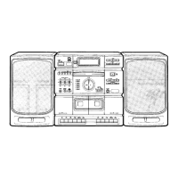
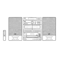
- 22 -
IC BLOCK DIAGRAM & DESCRIPTION
IC601 LC866548A (Micro Processor)
No. Name I/O Function
1 JOG+ I Input JogDial
2 JOG- I Input JogDial
3 D_CLK O Serial clock output for Tu/Vol_Func IC
4 D_OUT O
Serial date output for Tu/Vol_Func/extend IC
5 EXI_CLK O Serial clock output for extend IC1(DECK)
6 EX2_CLK O Serial clock output for extend IC2(LED)
7 EX3_CLK O Serial clock output for extend IC3(LED)
8 VF_CE O Serial latch output for Vol_Func IC
9 TU_CE O Serial latch output for Tuner IC
10 TU_DI I Serial date output for Tuner IC
11 O Not used
12 RESET I Reset terminal
13 XT1 I Sub clock connection terminal
14 XT2 O Sub clock connection terminal
15 VSS Ground
16 CF1 I Main clock connection terminal (6MHz)
17 CF2 O Main clock connection terminal (6MHz)
18 VDD Power supply (+5V)
19 KEY0 I Key input
20 KEY1 I Key input
21 KEY2 I Key input
22 CD_SW0 I SW input SW2(EXTRA) SW3(HOME)
23 CD_SW1 I SW input SW4(C_No.) SW5(C_No.)
24 CD_SW2 I SW input SW7(Fwd) SW8(Revs)
25 CD_SW3 I SW input SW6(Open) Pick Limit switch
26 LEVEL I LEVEL input
27 WRQ I CD DSP interface (sub Q Request)
28 PROTECTOR I Set protector (Irregular:Low)
29 IR I Remote control input
30 Digit13 O FL digit output
31 Digit12 O FL digit output
32 Digit11 O FL digit output
33 Digit16 O FL digit output
34 Digit10 O FL digit output
35 Digitl9 O FL digit output
36 Digit15 O FL digit output
37 Digit8 O FL digit output
38 Digit7 O FL digit output
39 Digit14 O FL digit output
40 Digit6 O FL digit output
41 Digit5 O FL digit output
42 Digit 4 O FL digit output
43 Digit3 O FL digit output
44 Digit2 O FL digit output
45 Digit1 O FL digit output
46 VDD Power supply (+5V)
47 Seg19 O FL Segment output
48 Seg18 O FL Segment output
49 Seg17 O FL Segment output
50 Seg16 O FL Segment output
51 VP FL drive output power
No. Name I/O Function
52 Seg1 O FL Segment output
53 Seg2 O FL Segment output
54 Seg3 O FL Segment output
55 Seg4 O FL Segment output
56 Seg5 O FL Segment output
57 Seg6 O FL Segment output
58 Seg7 O FL Segment output
59 Seg15 O FL Segment output
60 Seg14 O FL Segment output
61 Seg13 O FL Segment output
62 Seg12 O FL Segment output
63 Seg11 O FL Segment output
64 Seg10 O FL Segment output
65 Seg9 O FL Segment output
66 Seg8 O FL Segment output
67 SEL_RVS_A I
Tape Mechanism select
(Reverse=High, Normal =Low)
68 SEL_POW_RY I Power relay select (ON = high)
69 SEL_12_24 I Timer display (24h=High 12h=Low)
70 V_CHK I
Power suspension detection
Power suspention = Low/Micon power
75 B_PACK I
Tape set detection(B side) switch (ON=Low)
76 B_PALY I Play(B side) switch (ON=Low)
77 A_PACK I Tape set detection(A side) switch (ON=Low)
78 A_PLAY I Play(A side) switch (ON=Low)
79 A_REEL I Reel turn signal(A side)
80 B_REEL I Reel turn signal(B side)
81 POW_RY O Power relay control output (ON=High)
82 P_CON O Power control signal (Power on=high)
83 SP_RY O speaker relay control output
84 PRE_MUTE O PRE MUTE output (Mute on = High)
85 MAIN_MUTE O Main mute output (Mute on=High)
86 PULL_UP O pull-up power output (ON=Low)
87 DSP_RESET O Reset signal to DSP (CD)
88 CLK_SHIFT O Main clock shift
89 VSS Ground
90 VDD Power supply (+5V)
91 CARRIAGE+ O CARRIAGE-MOTOR control output+
92 CARRIAGE- O CARRIAGE-MOTOR control output-
93 DRAWER+ O DRAWER control output+
94 DRAWER- O DRAWER control output-
95 COIN O CD_DSP interface (command data output)
96 SQOUT I CD_DSP interface (SubQ data input)
97 CQCK O CD_DSP interface (clock)
98 VD_GND O GND control output for micon power check
99 DRF I DRF signal input
100 RWC O CD_DSP interface (command latch)
 Loading...