- 93 -
Electrical Adjustments
– 10 Fan D3 Min (✽) Fan D3 Driving Voltage Adj. at TPFN3 0 ~ 255 200 –
– 11 Fan D3 Max (
✽) Fan D3 Driving Voltage Adj. at TPFN3 0 ~ 255 50 –
– 12 Fan D4 Min (
✽) Fan D4 Driving Voltage Adj. at TPFN4 0 ~ 255 200 –
– 13 Fan D4 Max (
✽) Fan D4 Driving Voltage Adj. at TPFN4 0 ~ 255 50 –
S 141 – Fan Output Level
– 0 Fan Output Level 0 : Max / 2 : Auto / 3 : Min / 99: Menu 0 ~ 3 0 –
S 150 – Factory Set (Reset)
– 0 Factory Set Do not touched. Available at No.10 caution : Important! Do not attempt. 0 ~ 10 0 –
S 176 – Filter Display
– 0 Filter Icon display 0 : disable / 1 : Enable 0 / 1 1 –
S 177 – Filter Timer Reset
– 0 Filter Counter Reset Frequency User Menu Filter Counter Reset Frequency 0 ~ 255 0 –
S 180 – DDC Setting
– 0 HDCP EDID Data Setting 0 : EDID Data for DVI / 1 : EDID Data for HDCP 0 / 1 1 –
– 1 DDC Data Automatic Renewal 0 : Enable / 1 : disable 0 / 1 0 –
S 190 – Panel Life Test Pattern Display
– 0 Panel Life Test Pattern 0 : White 73% Raster Step Pattern Display / 1 : Normal 0 / 1 1 –
S 200 – Panel Option
– 0 Gamma Instance Gamma IC direct
(Gamma IC directed here is displayed by the
following service mode)
(900 / 910 / 920 / 940 / 950 / 951 / 952 / 960 / 970 / 9800 0 ~ 1 1 –
0 : 74h / 1 : 76h
S 280 – Panel Option
– 0 G SIG Center 0 ~ 63 32 –
– 1 B SIG Center 0 ~ 63 32 –
– 2 R SIG Center 0 ~ 63 32 –
– 3 G Gain Control 0 ~ 255 194 –
– 4 B Gain Control 0 ~ 255 194 –
– 5 R Gain Control 0 ~ 255 194 –
– 6 G Bright Control 0 ~ 255 0 –
– 7 B Bright Control 0 ~ 255 0 –
– 8 R Bright Control 0 ~ 255 0 –
– 9 G VCOM Control (
✽) 0 ~ 255 104 –
– 10 B VCOM Control (
✽) 0 ~ 255 104 –
– 11 R VCOM Control (
✽) 0 ~ 255 104 –
– 12 G SID Control A 0 ~ 255 16 –
– 13 B SID Control A 0 ~ 255 16 –
– 14 R SID Control A 0 ~ 255 16 –
– 15 G SID Control B 0 ~ 255 154 –
– 16 B SID Control B 0 ~ 255 154 –
– 17 R SID Control B 0 ~ 255 154 –
– 18 G FRINV 0 ~ 1 0 –
– 19 B FRINV 0 ~ 1 0 –
– 20 R FRINV 0 ~ 1 0 –
S 290 – Panel-LR
– 0 Panel Type _LR Read only 0 : Type - L / 20 : Type - R 0 / 20 0 –
– 1 Panel Type L/R _Chenge (
✽)Select Panel type L / R and Gamma Data Initialize 0 ~ 20 1 10
S 300 – CXD3815 - Common
– 0
– 1
– 2 CVBS Y Level CVBS / Y Input Gain Adjustment (Composite / S-VIDEO) 0 – 255 210 / 210 –
– 3 CVBS C Level C Input Gain Adjustment (Composite / S-VIDEO) 0 – 255 140 / 140 –
– 4 Sub Hue Tint Adjustment CVBS / S Input 0 – 63 32 –
– 5 HS Slice Level H Sync Slice Level 0 – 15 4 –
– 6 HS Slice offset H Sync Slice Level Offset 0 – 15 5 –
– 7 VS Slice Level V Sync Slice Level 0 – 15 6 –
– 8 VS Slice Level AD Clock 0 – 15 6 –
– 9 Sampling Phase V Sync Slice Level Offset 0 – 63 0 –
– 10 Pre Shoot Level Sub Sharpness 0 – 15 8 –
– 11 Over Shoot Level Sub Sharpness 0 – 15 8 –
– 12 Y Filter Setting Y Filter
Group 01 : Composite, S-Video 0 – 7 5/ –
Group
No.
Data
Range
Initial Value
Function
Item
No.
Item
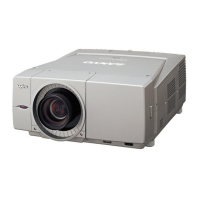
PLC-XF47
 Loading...