1234567891011 12 13 14 15 16 17 18 19 20
A
B
C
D
E
F
G
H
I
J
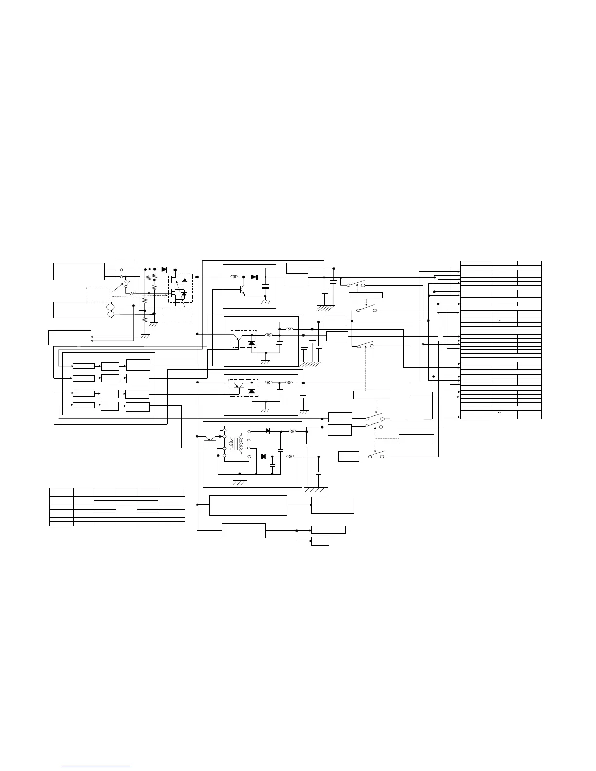
VE-CG30U
VE-CG40U
VE-CG30U
VE-CG40U
28~29
D1
*1: Only CG40 system for the AUDIO circuit and SP5V
Line name
Required spec
Connected to
Connected to
Connected to
Connected to
Connected to
Connected to
Connected to
Connected to
Connected to
ASIC
DPCON_1.8V
1.8 ± 0.1V
Vf2 APCON_5V
4.9 ± 0.1V
DPCON_3.3V
3.3 ± 0.15V
FET2 APCON_3.3V 3.3 ± 0.15V
Vf1 IO
FET1 APCON_5V
5.0 ± 0.1V
APCON_3.3V 3.3 ± 0.1V
MEM
DPCON_3.3V 3.3 ± 0.3V
SYSCON
DPCON_3.3V
3.3 ± 0.1V
SYS_3.3V
3.3 ± 0.1V
BATT_NONREG
3.6
7.5V
to SYSCON
CCD
CAM_-7V
-7.0 ± 0.3V
CAM_5V
5.0 ± 0.1V
CAM_3.3V
3.3 ± 0.1V
LENS
CAM_3.3V
3.3 ± 0.1V
LENS_3.5V 3.5 ± 0..1V
AUDIO *1
APCON_5V
5.0 ± 0.3V
APCON_3.3V
3.3 ± 0.3V
SP_5V 5.5 ± 0.3V
LCD
LCD_12V
12.0 ± 0.4V
LCD_3.3V
3.3 ± 0.1V
STROBE
NONREG
3.6
7.5V
APCON_5V 5.0 ± 0.1V
REG16V
REG-8V
Vf2: parasitic diode Vf2 of FET2 which is one of two FETs
Table 1. Operation of each section and the D/D converter input voltage by
plugging/unplugging the DC jack
Operation mode
BATT operation
Adaptor
operation
BATT operation
Plugging
Unplugging
Plugging/
unplugging the jack
DC voltage
FET1 ON OFF OFF OFF ON
FET2 ON
Batt BattBatt-Vf2 Batt-Vf2DC output
ON OFF ON ON
D/D IN
AC ADAPTOR
OUT: 6.0V – 7.0V (planed)
Electric current rating
(not yet determined)
Size AA battery, 4 cells
Voltage: 4.0 – 7.2V
(1.0 - 1.8V per cell)
DC JACK
OFF when the voltage
is applied to the DC
input
OFF when the DC
jack is inserted
5.5V booster circuit
5.5V
5.0V
REG circuit
4CH Power control IC
3.5V dropper circuit
Multi-transformer circuit
Constant current circuit for white LED
1.8V dropper circuit
DPCON_1.8V
15V
REG circuit
CAM_15V
CAM-7V
REG circuit
CAM 7V
APCON_5V
3.3V
RE