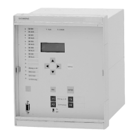
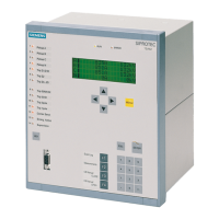
7SV512
Installation instructions
V1
45C53000---G1176---C91
5.2.4 Connections
General and connection diagrams are shown in Ap-
pendix A and B. The marshalling possibilities of the
binary inputs and outputs are described in Section
5.5.
Because of the high safety demand for the breaker
failure protection, a special trip release module is
provided for two of the trip relays. The operation of
this hardware logic module is described in Section
4.2.7.
Forthe trip release module to operate optimally, cer-
tain plug jumpers are to be observed on the addi-
tional p.c.b. EAZ---2. The trip release module and its
surroundings are shown in Figure 5.4. As delivered
from factory (= recommended positions) the binary
inputs BI 8, BI 9, and BI 10 must be assigned as
shown in Figure 5.4. The trip relays must be as-
signed such that trip relay K1 trips the bus-bar
breakers whereas trip relay K2 is intended to give
transfer trip signal to the opposite end breaker.
BI 9
General
trip
BI 10
Pl5
Pl4
”BFP TransTrip”
BI 8
Trip release module
&
&
&
Pl1
from processor
K1
General
start
External
block
Rel1
Rel0
Rel2
Pl2
Pl3
Trip
relays:
K2
”>Start
>Trip
>BFP block”
”BFP Trip BB”
Figure 5.4 Trip release module (hardware module)
Should the plug positions be changed for any rea-
son, the following is to be noted:
--- Ifone ofthe plugs Pl1orPl2or Pl3 is removed, the
corresponding AND condition is fulfilled!
--- The outputs ofthe AND---gates must not be paral-
leled by the plugs Pl4 and/or Pl5.
--- Nevertheless, it is admissible that the output of
the AND---gate Rel0 is connected to both trip re-
lays K1 and K2.
Pl1
X1 X2 X3
Pl2
X70 X71 X72
Pl3
X73 X74 X75

 Loading...

